New solar cells made more efficient

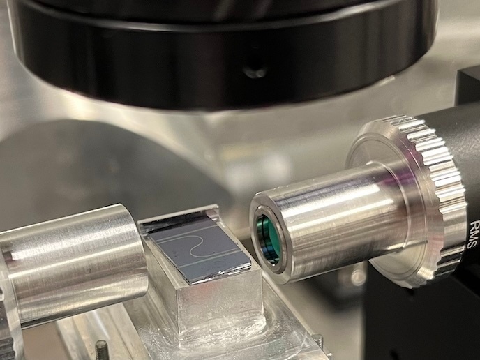
Currently, there is growing demand for small-format, semi-transparent or custom-shape PV cells. Repairing and reusing defective solar cells should provide the European PV industry with a competitive advantage. Funded by the EU, the project 'Repairing of photovoltaic wafers and solar cells by laser enabled silicon processing' (REPTILE)(opens in new window) provided the technology and methodology to transform cheap materials (scrapped cells and wafers) into small, custom and efficient PV cells and modules. The methodology employed promises higher efficiencies compared to that of the modules that are manufactured with standard solar cells. The concept is based on automatically recognising and classifying defects in C or D class cells. Then, automated laser processing is performed to obtain a smaller A class cell. Furthermore, a computer algorithm selects the optimal geometry to achieve maximum cell efficiency and minimum material waste. REPTILE's prototype system consists of a contactless laser system that cuts and isolates non-defective parts. A vision system and software were developed for detecting the defects and provide the laser repairing system with the required automation and flexibility degree. Another prototype key component is the automated characterisation system that is integrated with the laser system. A powerful luminescence and thermography combination was tested for detecting and characterising all significant defects with enough spatial resolution to feed the repair system. Furthermore, a novel gripper design was developed to automatically separate cells during the sorting phase and feed the repaired and modified cells again in the manufacturing line. By using the project prototype, project members built proof-of-concept modules from the repaired solar cells and evaluated their repairing process effectiveness. Modules produced from repaired cells proved to have equivalent or even better performance compared to standard A class cells. The project successfully bridges the gap between the European PV market and the small and medium-sized enterprises (SMEs). Rejected cells and wafers end up being reprocessed, thus opening the door to new markets for SMEs.