Silicon takes the strain
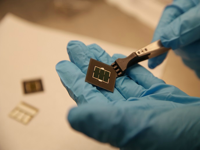
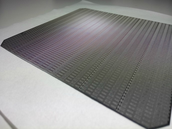
Voided structures in strained Si offer a unique opportunity to exploit their bizarre properties in photovoltaic (PV) applications. Through irradiation with light ions, strained Si — accomplished by putting silicon-germanium (SiGe) and Si layers over a substrate of silicon — results in nanodot and nanovoid formation. Their unusual electronic and optical properties have not been hitherto experimentally studied in solar cell configurations. The EU-funded project 'Nano-voids in strained silicon for plasmonics' (NOVOSIP) offered a unique PV device configuration to study void-containing Si/SiGe-strained structures. Scientists sought to place nanodots and nanovoids in a highly doped emitter layer close to the p-n-junction to extend near-field effects to the depletion region. These effects would then give rise to carrier multiplication and increase light scattering due to far-field effects, both being promising for enhancing sunlight absorption. Researchers used different methods to investigate the structural, optical and electronic properties of the periodically formed strained layers. The plan was to use the findings to prepare plasmonic structures for Si-based PV devices, solid-state gas sensors and optoelectronic devices. Through high-temperature ion irradiation of the Si/SiSn/Si structure, scientists obtained self-assembling spherically shaped nanovoids and strained tin (Sn) precipitates. These structures hold great promise for optoelectronic applications such as light-emitting or PV devices. With carbon ion implantation and thermal treatment, scientists observed carbon nanoflake formation in the strained multi-layered Si/SiGe/Si structure . The flake crystalline structure allows the crystals to absorb all light, potentially allowing a very high energy conversion rate. The team developed and proposed a new concept for self-assembling of metallic nanoshells and nanoparticles in the strained Si/SiGe heterostructures . The metallic nanoshells can be further investigated in solar cell structures to demonstrate plasmonic effects. Finally, NOVOSIP demonstrated gas-sensing effects related to plasmonic structures in a nanocomposite layer based on Sn dioxide (SnO2) with voids. High efficiencies in addition to low costs are the main design challenges in fabricating solar cells. With experimental investigation of plasmonic structures in strained silicon multi-layers, NOVOSIP paved the way to enhancing light harvesting in solar cells.