Small diamonds with big industrial impact

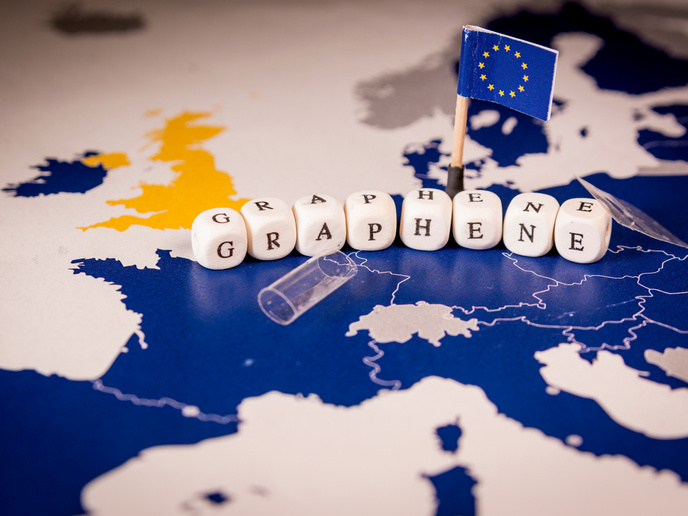
The EU funded the Marie Curie International Research Staff Exchange Scheme (IRSES) project CARBONNASA (Carbon-based nanomaterials and nanostructures for advanced sensing applications). The project brought important skills and expertise from China, Japan and the United States to European labs equipped with the infrastructure to exploit them. It was designed to support knowledge transfer regarding nanomaterials that will facilitate development of potentially groundbreaking technologies and devices currently not available in Europe. Applications abound in fields from energy to biomedicine to microelectronics. Researchers focused much effort on fabrication of high-quality diamond thin films, both homoepitaxial (diamond on diamond substrate) and heteroepitaxial (diamond on another substrate). Using femtosecond laser irradiation, the team demonstrated for the first time the feasibility of creating microfluidic channels on a biocompatible single-crystalline diamond substrate. The pioneering work was published in Applied Physics Letters. CARBONNASA also synthesised novel carbon nanofibres that can be used to facilitate bone growth and research into antimicrobial resistance. The strong luminescence properties of certain fibres also prove attractive for applications in optoelectronics. Diamond exceptional surface chemistry and mechanical properties were exploited for the development of devices devoted to pressure sensing. Researchers successfully developed a self-integrated metal-piezoelectric-insulator-semiconductor field-effect transistor, a high-sensitivity microelectromechanical device for detecting pressure at high temperatures. Numerous point defects in diamond, keenly explored for their photoluminescence properties, can be turned into quantum emitters. The team fabricated arrays of diamond nanostructures of different diameters and top end shapes with embedded nitrogen-vacancy centres. These point defects emitted single photons 10 times more efficiently. Another area of development was the application of nanomaterials to lithium battery technology. Scientists demonstrated significant improvements in performance and storage properties using a variety of newly fabricated materials. The plethora of advances led to four more publications. CARBONNASA was a unique multidisciplinary, multi-continent research staff exchange project leading to amazing new developments in the field of next-generation carbon-based nanomaterials and devices. Results are pouring in and expected to have important impact on fields including biomedicine, nanotechnology, optoelectronics, sensors and energy. With its broad technology training and application spectrum, project work will support the EU's transition to a knowledge-based economy.