EU leadership in printed electronics
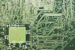
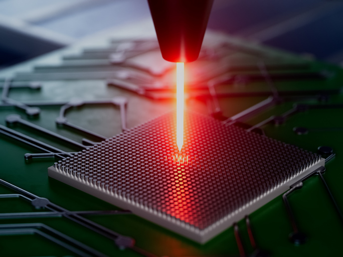
PCBs rely on conducting inks printed onto hard substrates to connect 3D components that are soldered to the board, creating electronic circuits. The concept is about to make an evolutionary leap with new technology that is rapidly entering the market. Printed electronics exploit conductive and dielectric inks to make thin-film transistors (TFTs) that can be printed over large flexible substrates with low-cost, high-throughput methods. Growth rates are expected to be comparable to those of the silicon industry in the past, achieving a market size of USD 47 billion by 2018 and an amazing 300 billion by 2030. In support of Europe's goal to achieve world leadership in the strategically important printed electronics sector, the EU funded the POINTS(opens in new window) (Printable organic-inorganic transparent semiconductor devices) project. Scientists targeted breakthrough advances in new low-temperature printable materials. The team took advantage of the processing benefits of organic (polymer) materials and the superior properties of inorganic (metal oxide) ones by creating advanced hybrid materials. The performance of solution-processed organic TFTs has surpassed that of thin-film amorphous silicon TFTs. However, inorganic semiconductors and insulators have superior properties over organic ones and metal nanoparticle inks are much more conductive than conducting polymers. Metal oxide-based polymer-encapsulated nanoparticles were used to produce printable semiconducting and insulating materials for TFTs. In particular, solution combustion synthesis was used to fabricate n-type oxide semiconductors at lower temperatures than required for conventional sol-gel processes. The method was also used to fabricate dielectrics. Simple logic flip-flop circuits, ring oscillators and light-emitting diode (LED) drivers were implemented with the new materials. They were incorporated into an interactive card demonstrator in which blinking LEDs that represent the Ursa Minor stars are turned on and off by the user. Although the focus was on information and communications technology, the technologies can easily find applications in other areas, including displays, lighting and photovoltaics. POINTS outcomes resulted in two patent applications and have been widely publicised in scientific journals and at conferences. The team expects the project to have a catalytic effect on EU printed electronics, pushing Europe ahead of its American and Asian competitors in a huge global market. A video of this application is available online(opens in new window).