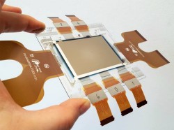
Novel hybrid nanostructures for quantum computing
Within COSPINNANO (Coherent spin manipulation in hybrid nanostructures), researchers have fabricated hybrid nanostructures to probe the various processes that govern spin dynamics in these systems. They evaluated using top-down and bottom-up approaches to nanofabrication – electron beam lithography and atomic self-assembly, respectively. The first activity was to prepare suitable nano-scale junctions for innovative device technologies such as memristors that allow realising compact non-volatile memories. Researchers successfully controlled resistive switching in Ag2S-based memristive devices and demonstrated high-speed switching in room-temperature conditions. Using point-contact Andreev reflection spectroscopy, they explored the nature of electron transport in the active volume of memristive junctions. The study revealed that ON and OFF states correspond to truly nanometre-scale, highly transparent metallic channels. Another area of focus was on cutting graphene nanoribbons and depositing nanocircuits on them. Hybrid nanocircuits based on carbon and a semiconductor require highly conductive lead wires that are compatible with metallic, superconducting and ferromagnetic terminals. Researchers observed high electron transport rate values of the fabricated graphene nanoribbons. Graphene nanoribbons designed for such purposes were fabricated and tested in the wide temperature range of 1-300 K. This finding has demonstrated that these graphene structures can be successfully used as basic building blocks of multifunctional nanodevices. Experimental activities also included spin measurements of quantum point contacts implemented in low-dimensional semiconductor systems (gallium arsenide/aluminium gallium arsenide heterostructures). This work contributed to better understanding the influence of the confinement potential on spin orientation in the adjacent 1D electronic sub-bands. Moreover, the team studied the origin of conductance anomalies in these quantum point contacts. Novel hybrid nanostructures provide the opportunity to study electron charge and spin dynamics in multifunctional devices. These include fast-switching devices, combined logical and storage devices, and semiconductor spin qubits based on quantum dots. Project results also help determine a path to manipulating the spin of single electrons – a daunting technological challenge that will, however, lead to new paradigms in quantum information processing.


