Tips for high-resolution imaging

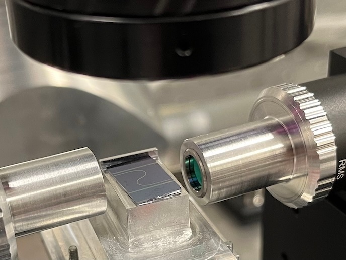
Shortly after the invention of STM, it was discovered that only sharp tips can provide stable and reliable imaging of atomic reconstructions on metallic surfaces. The ultimate resolution can be reached with tips collecting most of the tunnelling current through electron orbitals of a single atom at the apex. STM tips are usually prepared from low-cost polycrystalline tungsten wires using electrochemical etching. Picoscale resolution can also be achieved using tips made of light-element atoms. However, most tip treatments do not produce stable apexes with well-defined atomic and electronic structure. The controlled fabrication of tips suitable for STM experiments was one of the main issues addressed by EU-funded scientists. The ultimate objective of the project ORBITAL IMAGING (Electron orbital resolution in scanning tunneling microscopy) was to improve the imaging of metallic surfaces with complex structures. The ORBITAL IMAGING team prepared [001]-oriented tungsten probes sharpened in ultra-high vacuum using electron beam heating and ion sputtering. Both scanning and transmission electron microscopy confirmed reproducible fabrication of the single-atom tips with nanoscale pyramids grained at the apexes. Next, the researchers demonstrated the advantages of these single crystalline tungsten tips for STM imaging of pyrolytic graphite, silicon carbide and graphene surfaces. Importantly, a direct relation was found between the tip structure and picoscale resolution achieved in these experiments. The single crystalline tungsten tips were also used for high-resolution STM imaging of regularly stepped silicon surfaces. Under precise thermal treatment, the selected surfaces reconstruct into atomically accurate arrays of silicon terraces and triple steps with equal height. This unusual surface reconstruction became the subject of extensive research in ORBITAL IMAGING. Using high-resolution STM data obtained with tungsten tips of high stability, the researchers found that periodicity on grooved silicon surfaces can be maintained and proposed a model of their atomic structure. ORBITAL IMAGING results revealed picoscale resolution achieved in STM experiments with tungsten probes that are comparable to the highest resolution obtained so far in scanning probe microscopy. Moreover, the experimental studies confirmed the suitability of graphene grown on silicon carbide wafers for nanoelectronics.