New semiconductor materials for smaller and more powerful devices
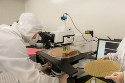
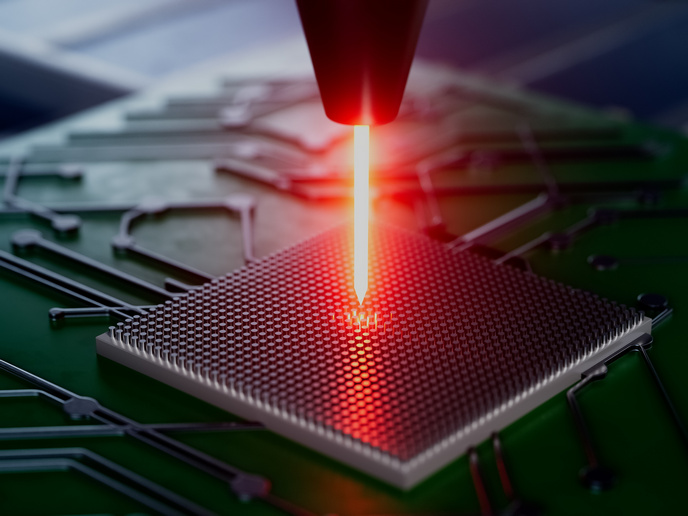
The ongoing impact of Moore’s law has been driving advances in computing devices as they keep getting smaller, faster and cheaper. Thus, the semiconductor industry is facing the challenge of how to migrate processes that were once developed for some few microns to be able to form junctions that are a few nanometres in scale. Within the EU-funded project FACIT (Fast anneal of compound semiconductors for integration of new technologies), scientists successfully combined III-V materials – indium, gallium and arsenide (InGaAs) – with silicon germanium (SiGe) technology to create CMOS chips. The newly developed process is compatible with high-volume chip fabrication, making it a viable option for chip manufacturers. Using the same large-sized Si wafer of 350-400 mm, the project team developed a process that allows integrating InGaAs, SiGe and Si CMOS layers. Scientists considered this method as a means of further shrinking and scaling CMOS technology at a nanometre level. The material properties of SiGe and InGaAs are very different from Si, particularly with respect to thermal treatment. Furthermore, InGaAs and SiGe require very different processing conditions in terms of thermal budget. Ultrafast annealing is a key technology for enabling the co-integration of SiGe and InGaAs. FACIT scientists further explored millisecond annealing of high-mobility channels. Results proved that the use of millisecond annealing can drastically reduce the interface state density, and as a process is equivalent to a conventional one, but using a substantially lower thermal budget. Ultrafast annealing can serve to form stable shallow junctions. Project results are promising since replacing silicon with high-mobility channels such as Ge and InGaAs will be the next major materials revolution. Integrating such high-quality materials on Si is important for building transistors with improved power and performance at a nanometre scale.