

No limits to silicon integrated circuits
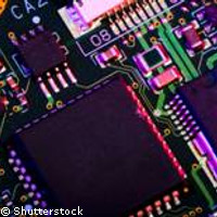
Microchip processing technology is being updated at faster and faster rates in our age of silicon chip wizardry. By the time you unpack your smart new laptop or digital camera, the technology that went into making it is already becoming outdated. But a solution to the problem is now at hand. Researchers working on a project called PICMOS, with EU funding of €2.5 million, have developed new technologies to produce and combine semiconductor microlasers with silicon wave guides for new, efficient and powerful optical connections. Traditionally tiny copper wires connect different areas of integrated circuits, but these are limited in their use as they will soon start limiting microchip processing speeds. Since the birth of microchip technology, the miniaturisation of microchips has continued relentlessly, with the number of transistors that can be fitted into an integrated circuit doubling on average every two years. Microchips that are based on silicon wafers are now nearing their limits because the physical properties of near nanoscale silicon integrated circuits are beginning to interfere with their performance. The speed of data transfer in the integrated circuits is slowing down because the data is currently being sent as electrons through copper wires known as copper interconnects. 'Copper wire interconnects place serious limitations on the performance of silicon integrated circuits,' Dries Van Thourhout from Ghent University's Photonics Research Group and Belgium's IMEC, a micro- and nano-electronics research centre, told ICT Results. 'It is hard to transmit data down these interconnects in a sufficiently fast power-efficient way. It is a problem of bandwidth and copper will not be able to cope with the processing power of tomorrow's microchips.' Using optical connects would be far more convenient than copper ones as opticals use light instead of electrons to relay data. They also have the capacity to be far more efficient at transmitting data, but using the same or less power. Instead of travelling along copper wires, they travel along wave guides that are made of silicon rather than glass. 'Lots of research has shown that you can etch wave guides for photons into silicon,' Dr Van Thourhout is quoted as saying. 'This is great because you are using the same materials and fabrication technologies as you do to make integrated circuits. But there is one significant drawback: it is extremely hard to get light out of silicon.' Part of the project research involved the development of indium-phosphate lasers etched with a diameter of just 7µm, which is small enough to integrate several thousand onto a 2cm x 2cm silicon chip. These could be used in many ways, for example in miniature optical sensors such as strain detectors. Or they could be used to build inexpensive, but powerful optical biosensors. At the moment the cost of producing the lasers is too high for mass production, although the results of the research are encouraging. A follow-up project called WADIMOS, also EU-funded, is to carry on the PICMOS research.