Nanonet-based sensors for medical applications

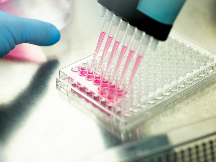
In medicine, biosensors are used to detect a particular chemical biomarker, or a DNA sequence that causes diseases or is associated with susceptibility to a disease. Currently, DNA molecules can only be quantified using centralised and often expensive tools. Being able to provide point-of-care monitoring, using low-cost devices, would allow for a more reactive follow-up of tumour evolution, more personalised treatments, and better patient care. To help make biosensors applicable to the point-of-care setting, the EU-funded Nanonets2Sense project explored the potential use of nanonets for the 3D integration of biosensors on a technology for making low-power integrated circuits called complementary metal oxide semiconductors (CMOS). “Today’s DNA biochips are usually based on a labelling technique where the DNA molecules of the biosample being tested are first tagged by fluorescent labels so their immobilisation with the proper probe can be visualised,” explains Mireille Mouis, a researcher from the French National Centre for Scientific Research (CNRS) and Nanonets2Sense project coordinator. “R&D activities now focus on label-free methods where the interaction between the target and the probe molecules is directly sensed through the modification of the electronic, optical or mechanical properties of the transducer.”
A compact device
Nanonets are random arrays of thin and long nanostructures called nanowires(opens in new window). According to Mouis, it was recently discovered that nanonets made of silicon or zinc oxide nanowires could be fabricated and made conductive using a low-cost, bottom-up process. The resulting material, which is semiconducting, can be used as an active material for biosensing applications. “Using this fabrication process, we created devices showing some key features of the promising nanowire-based sensors, but without the cost of integration that has hampered their development for use with sensing applications,” explains Mouis. The compact device places the sensors on top of the readout circuit, thus putting the sensors in direct contact with the biomolecules being detected. This design not only ensures that the readout and conditioning electronics at the silicon CMOS level are protected from fluid, it also means they can be connected vertically through the backend of the CMOS wafer. This allows compact routing, which in turn allows for the readout of possibly large matrices of sensors – a feature that can improve the reliability of the detection.
Charting a new course
Starting from a very simple technology, the Nanonets2Sense project has successfully created and validated all the innovative technological building blocks needed to enhance CMOS chip functionality with nanonet-based biosensors. The readout scheme is also new. “Prior to this project there had been virtually no attempt to develop point-of-care devices based on silicon or zinc oxide nanonets – the field was mostly uncharted,” says Mouis. “Our ultimate goal was to realise full 3D integration of biosensors on CMOS and we now have the technology needed to complete this integration in an industrially relevant context.”