Fantastic particles and where to find them

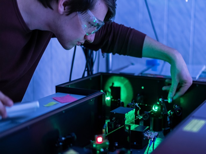
Typical activities in ordinary life consist of sending and receiving information. The news or notifications we see on smartphones, from magazine gossip to football scores, reach the device from a domestic Wi-Fi router or mobile phone mast, which receives input from a giant server network disseminated across the world. Zooming in the path, two particles are information vehicles: photons, from servers to devices, and electrons inside the devices. These two communication mechanisms require different hardware platforms that, when combined, are often inefficient and dissipate energy. Could scientists improve on this process by producing more stable channels for information? The TOCHA project is trying to send information with the smallest waste of energy by identifying efficient channels at the nanometre scale – one billionth of a meter. Set across nine European research institutions, the project is coordinated by the Catalan Institute of Nanoscience and Nanotechnology (ICN2) and funded by the EU’s FET (Future and Emerging Technologies) programme. Material worlds There are two main lines of research in the TOCHA programme, the electronic (namely the Physics and Engineering of Nanodevices group) and the photonic ones (the Photonic and Phononic Nanostructures group). The electronic group activity begins by modeling the material to study. “We grow the nanofabrics using a technique called molecular beam epitaxy,” explains Iván Fernández Aguirre, a doctoral student at ICN2. “In plain speaking, it’s like cooking: mixing several chemical elements ingredient, like tellurium or bismuth, with particular temperature and pressure conditions.” The sample grows, layer after layer, following a precise model, a sort of mold. The ultimate purpose is not just to grow something, but something with useful and interesting characteristics to analyze. The class of materials researchers are focused on, because of their electrical properties, are topological insulators: materials within which electrons can exclusively move along the surface of the materials, not in other parts. On the grown nanofabric, which appears like a continuous sheet, scientists “draw” the channels on which they want the electrons to travel. “This process is called photolithography and uses some chemicals very sensitive to light. It’s very similar to the old way to develop films, in the darkroom,” says Adriana Isabel Figueroa García, a postdoctoral researcher at ICN2. It takes place in a super clean room, where special suits and masks are needed to enter and work in so as to avoid introducing outside pollutants into the ultra-clean environment. The last step of our sample itinerary requires electronic tests. To examine how the new material performs at varying temperatures (sensitive to the order of millikelvin), electrical currents and magnetic fields, to better understand how the material will behave in the final devices we might one day use to send and receive our texts, pictures and calls. The power of analogy On the other hand, the work chain for photonic researchers is similar to the electronic ones, but with some differences. “Analogies are a very strong tool in physics, so we try to apply the idea behind the electronic nanofabrics and generalise it to photons and other particles, using the knowledge we already understand,” says Pedro David García Fernánde, a postdoctoral researcher at ICN2. The main variation between electronic and photonic technology involves the channel fabrication: for photons they are made through the shape of the nanofabrics, not by drawing on the materials but with specific geometries, like crosses or periodic holes on the surface, to guide and force how light is emitted and transmitted. Final tests then clarify what kind of geometries are the most valuable at the nanoscale. Read the full article on http://www.fetfx.eu/story/fantastic-particles/(opens in new window)