Micro-printing presents mega advantages
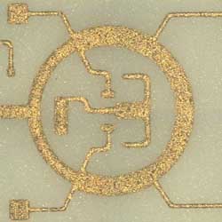
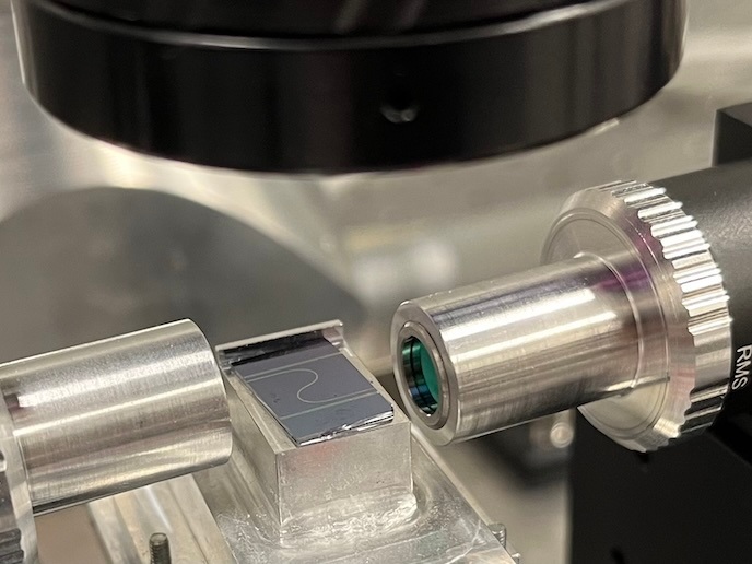
Conventional circuit board printing requires extremely high tech procedures that can produce tracks and spaces between tracks of up to 200 micro-metres. These are procured through the use of thin-film technology, a highly expensive resource which requires the additional treatment of precision laser trimming. Using standard screen frames, a stainless steel foil micro-etched with ink-feeder holes and having a underlay of organic gasketing to ensure ink-flow accuracy, the micro-Screen produces thick film track definition to an astounding micro-tracking of 50 micro-metres. It therefore, reduces the need for laser trimming, track multi-layering and hence, offers screen print manufacturing significant advances without major capital outlays. The micro-Screen allows for unique patterning of circuitry through standard CAD design programs effectively permitting each micro-Screen foil mesh to be unique and tailor designed. Because it requires no special engineering, micro-Screen can utilise thick-film technology, standard printing processes and produces far better results than thin-film and photo-imaging techniques. This technology, currently ready for demonstration, has shown best results with microwave circuits, reducing the need for high-tech interconnect components, improving track edge definition and enhanced circular or radial tracks that do not have random edge effects associated with current printing technologies. Micro-Screen may be making minute tracks in screen printing, but with all the advantages it presents, it should promote considerable benefits to micro-printing technologies. More information can be found at: http://www.era.co.uk/microscreen.htm(opens in new window)