Imaging materials on a fine scale
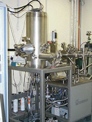
Modern scanning probe microscopy and microanalysis covers extremely powerful and high-resolution technologies for imaging and measuring materials on a micro scale, down to the level of molecules and groups of atoms. Among them, the 3D atom probe (3DAP) is the most popular instrument for the analysis of metallic alloys. However, due to the great difficulties of producing specimens in the correct form for further analysis, it has limited applications in the fields of thin film materials and surfaces. Motivated by this, a consortium of experts in the design and manufacture of scientific instrumentation with end user applications, resulted in the development of a unique scanning atom probe (SAP). Combining special techniques, the SAP facilitates the fabrication of thin film specimens in the form of microtips that are used for further analysis. Furthermore, the system allows better characterisation of the chemical and physical properties of materials on the nanometric scale with increased precision, even in the uniquely unstable microworld. Apart from the specimen tip system, the SAP instrument exploits an innovative counter electrode that allows not only an enhanced mass resolution, but also the previously impossible identification of single atoms even in materials with elements close together in the mass spectrum. In addition, a new delay line position detector is used for optimised sensitivity that with the aid of specialised hardware (data acquisition and pulser) has the potential to observe fast data rates of up to 300 ions per second. The SAP is user friendly and offers its users full control of the positioning and scanning procedures. It has been extensively tested for preliminary studies of metallic multilayer films, for producing silicon specimens and for measurements of the degradation of phosphors used in display technology. Most importantly, it may become a routine user instrument for a range of materials problems. Bearing in mind the growth of nanotechnology in Europe, it is anticipated that the SAP instrument will provide a valuable asset for advances in the development of nanostructured materials.