Low cost packaging of micro-electromechanical systems
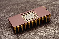
MEMS are expected to play a vital role to the development and expansion of intelligent devices. However, compared to regular integrated circuits (ICs), they are more complex due to the interactions taking place between their diverse components and their stern packaging requirements. The packaging of MEMS devices is a critical factor to both their functional behaviour and production cost. The packaging scheme must provide protection during dicing and against environmental conditions such as moisture or pressure. Due to the broad diversity of MEMS basic building elements, their packaging is mainly application specific and can not be applied to a wide range of devices as a generic process. Currently, the procedures employed for the packaging of MEMS are based on wafer level operations. Such processes involve wafer bonding where two semiconductor wafers are bonded to form a substrate with desired properties or alternatively involve the fabrication and sealing of surface micro-machined membranes over the device that needs to be encapsulated. These methods, though effective, are expensive and area consuming. The SUMICAP research project aimed at developing a wafer encapsulation technique which would remove the current limitations, emphasizing on cost savings. SUMICAP led to a broad range of processes for the packaging of MEMS via encapsulation, giving promising results and providing significant know-how to the field. This was achieved through the thorough evaluation of possible processes such as deep silicon etch, silicon germanium (SiGe) etch or boro-phospho-silicate glass (BPSG) deposition. In addition, two new processes based on BSPG and Plasma Enhanced Chemical Vapour Deposition (PECVD) respectively have been developed, which are expected to have an immediate impact on packaging technologies. The implementation of the resulting processes and the exploitation of the know-how gained, will open new trails on the commercialization and wider use of MEMS devices, due to the reduction in packaging costs. This would not only lead to the production of new and more sophisticated equipment but also to an improvement in quality of life.