

EU researchers develop efficient new nanowire analysis technique
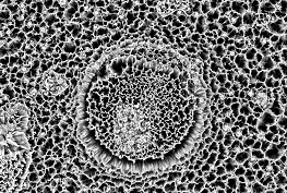
Researchers working through the EU-funded NANOWIRING project have developed a new cost-effective and time-efficient technique for determining the individual polarity of semiconducting nanowires. This is a vital step in the fabrication of nanomaterials, since the polarity – whether nanowires are positively or negatively charged – defines the properties of any device made from these cutting edge structures. Semiconducting nanowires are just tens of nanometres in diameter with a typical length-to-width ratio of around 1000; like a human hair, only a thousand times smaller. Due to their size and almost one-dimensional nature, interest in fabricated semiconductor nanowires has been growing steadily. For example, they are the smallest dimensional structures that allow optical guiding and electrical contacting simultaneously. Their large surface to volume ratio also enhances their interaction with the environment, turning them into optimal chemical and biological sensors. In addition, their geometry makes their optical and electrical properties dramatically dependent on their orientation, allowing their use as polarisation-dependent sensors. To this end, the project studied possible applications in quantum information processing and novel optical-electronic devices. Light-Emitting Diodes (LEDs) based on single nanowires were developed, and were shown to offer highly efficient conversion of electron-hole pairs into photons. The new technique developed by NANOWIRING uses an atomic-strength microscope and a Kelvin probe to detect minuscule forces, and measure the electrical characteristics of the sample’s surface. When combined with advanced data analysis, these measurements reveal the polarities of hundreds of nanowires at the same time. Up until now, determining polarity required nanowires to be analysed one-by-one as part of a complex and time-consuming process. This means that what used to take days can now takes a matter of hours, without any damage to the sample. This development has been a key result of the NANOWIRING project, the overall objective of which has been to create a European network of experts to provide assistance to early stage researchers. Starting in 2010, a pool of postgraduates and young researchers were embedded in multidisciplinary research and development activities, focused on tapping the industrial potential of semiconductor nanowires. An advanced school on semiconductor nanowires covering a broad range of topics from fundamental physics to device applications was held in 2013 in Italy. International experts provided a comprehensive overview on fundamentals, recent progress and approaches to solving open questions in the growing field of semiconductor nanowires. The scope of this project, which has now been officially completed, has also been very much driven by industrial needs, such as achieving scalable and low cost nanowire production. Industrial partners have been involved throughout in order to ensure that research and results are as market-focused and applicable as possible. Furthermore, interaction with associated industrial partners will enhance the employability of researchers through exposure to the private sector. For further information please visit: NANOWIRING project website(opens in new window)
Countries
Germany