Water splitting made easier
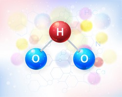
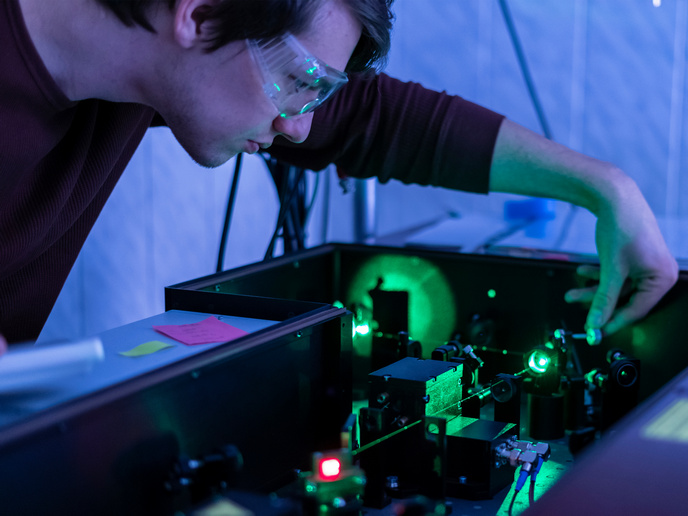
The Z-scheme is a process by which photosynthesis in plants splits water into hydrogen and oxygen using light. The Z-scheme consists of two photosystems, abbreviated as PSI and PSII. Electrons removed from water in PSII are transferred to the highest occupied molecular level of PSI. While the photogenerated electrons in PSI participate in reduction of protons to produce hydrogen, the holes in PSII oxidize water molecules, producing oxygen. The EU-funded HETMAT (Heterostructure nanomaterials for water splitting) was an initiative to synthesise nanomaterials for water splitting through an improved, rational design process. Researchers designed a system mimicking the efficient water splitting process of photosynthesis in green plants. HETMAT mimicked this so-called Z-scheme expecting to generate hydrogen much more efficiently. To successfully design novel nanomaterials, the researchers made several changes to the current Z-scheme. To meet important technical requirements, HETMAT engineered an interface between two different nanomaterials and then synthesised a single material. The researchers further modified the Z-scheme by selectively depositing metal nanoparticles on semiconductor phases. HETMAT explored various semiconductor materials and used some in the form of nanostructured thin films while others they used in the form of nanoparticles. The researchers studied materials such as zinc oxide (ZnO), silver decorated ZnO, tungsten trioxide, iron oxide, copper oxide (CuO) and others. Most important to the study, the researchers took a unique approach to the fabrication of copper halogenide thin films and their conversion to CuO thin films. HETMAT demonstrated for the first time the electrodeposition of copper chloride thin films and filled missing details in the literature. Going beyond the exploration of efficient photocatalysis through known semiconductors, the researchers discovered a novel semiconductor based on lead tellurium vanadate. The researchers developed this material that can be used for many applications, including cation or anion doping. The low synthesis temperature can be an advantage for industry applications where low processing temperatures are required. These results will boost the photocatalytic activities of nanomaterials for overall water splitting by attaining a quantum yield above 6.3 % at 420 nm. This work will be commercialised through templating systems combined with wet-chemistry synthetic routes to prepare nanomaterials more easily.