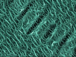
New research into one-dimensional nanowires
1D semiconductor nanowires promise to provide the building blocks for a new generation of nanoscale electronic and optoelectronic devices. Based on their distinct optical, electronic and magnetic properties, they make ideal candidates for a wide range of applications, including photovoltaics, piezoelectrics, thermoelectrics, lithium-ion batteries, field-effect transistors, photodetectors, light-emitting diodes (LEDs) and lasers. The EU-funded project NANOEMBRACE(opens in new window) (Embracing one dimensional semiconductor nanostructures) brought together 10 academic and 12 industrial research teams. They conducted a series of interconnected research into controllable growth of 1D nanostructures, controlled modification of 1D nanostructure composition to form quantum wire heterostructures, non-destructive characterisation of 1D nanostructure arrays, and functionalisation and interfacing of as-grown 1D nanostructures. Researchers experimented with different methods for growing ensembles of semiconductor nanowires with predefined shape, dimensions, direction of growth, crystal structure and substrate position, exploiting use of different substrates and catalysts. Researchers’ activities ranged from the investigation and modelling of fundamental mechanisms of nanowire growth to the fabrication of device samples. In particular, researchers developed a multi-scale platform characterisation to map structural, electrical and optical properties of individual nanowires and ensembles as well as nanowire-based devices. The effort was supported by high-resolution microscopy and advanced optical analysis methods. Functionalisation of 1D nanostructures helped researchers capitalise on the achievements in theory, growth and characterisation, and to demonstrate new instruments, sensors, optoelectronic and energy conversion devices. Therefore, exploiting the intriguing properties of these nanowires, the NANOEMBRACE team successfully demonstrated nanowire-based high-sensitivity and high-resolution scanning thermal microscopy, organic vapour sensors based on DNA-templated nanowires, nanoscale porous silicon microtubes in LED architecture, highly sensitive pressure sensors of wide dynamic range and components of a tandem solar cell. Project results helped create greater awareness of nanowire research and technologies. This was evidenced by the sheer number of participants at project workshops and conferences. Results can also be found in numerous publications in high-impact journals and on the project website.


