Taking guesswork out of industrial crystal production
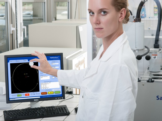
Synthetic sapphire is commonplace in everyday life, as its optical, mechanical, thermal, chemical, and structural properties are highly valued in a vast array of fascinating applications. For example, the material is used in wristwatch crystals, surgical systems, as a component in defence and aerospace applications and as a substrate for solid-state electronics, such as white light-emitting diodes (LEDs). However, despite the strong commercial need for it, growing the material reproducibly to the highest grade is not that simple. With EU funding of the SAPPHIRO project, Scientific Visual has been able to identify and quantify internal defects in sapphire at earlier stages in the production cycle than previously possible. Its new system helps address the lack of international quality standards, which ultimately creates uncertainty in end users about the quality of product they are buying or selling. Making the invisible visible Scientific Visual developed the first-ever systems to identify internal flaws reliably in unpolished sapphire. The new automated quality control scanner called SapphiroScan™ visualises and analyses volume defects including bubbles, cracks, cloudiness, inclusions and lattice distortions in raw sapphire. The technology is ideal for identifying imperfections in pre- and post-polished sapphire watch covers, ingots and wafers. “SapphiroScan™ relies on refractive-index matching of different liquid and solid substances to improve the overall optical clarity. This data is combined with tomography and image processing software that renders in 3D the detected material defects. The new automated inspection technology is non-destructive and accurately maps all the defects, regardless of their type, size, and location in industrial crystals,” explains Ivan Orlov, founder of Scientific Visual. Importantly, manufacturers know in advance where defects are located and therefore decide how to best exploit the material. Saving time and costs Industrial crystals just like sapphire and silicon carbide have remarkable hardness close to that of diamond – this is making it difficult to produce large quantities of fine quality. Expensive slicing, grinding and polishing machines are used all day long to produce the final object. “Currently checking for defects in semiconductor wafers, or watch and smartphone camera covers is only conducted after full processing and polishing has been completed. Given that approximately 10 to 15 % of watch covers are rejected after processing due to flaws, a typical sapphire factory wastes at least half a day per week polishing discards,” outlines Frédéric Falise, COO of Scientific Visual. Another inspection system, SapphiroScope™, detects flaws in sapphire for the semiconductor industry prior to its grinding and polishing, ensuring that only high quality material enters the LED value chain. The scanner not only allows materials to meet quality standards but also reduces production time and costs. Offering a fast, highly cost-effective alternative to manual quality control, it helps increase the production yield and saves up to 15 % of overall industrial operation costs. Together with metrology and wafer inspection, defect review, analysis, and classification are vital in crystal production, providing the means to monitor and control the quality of individual steps in the crystal manufacturing sequence. Scientific Visual aspires to reshape current market practices on synthetic crystal processing, setting its disruptive technology as a global industry-wide cross-application standard. By 2022, its technology will allow for reducing the industrial crystal defect rate by a factor of two. Thanks to Scientific Visual’s technology, the higher crystal yield will ramp up electronics production, especially for renewable energies, electrical vehicles and LEDs. The company is open to partnering with other industrial players to license its technology in specific market verticals such as precision optics, glass and laser ceramics inspection.


