Novel 2D material design for more stable electronic inks

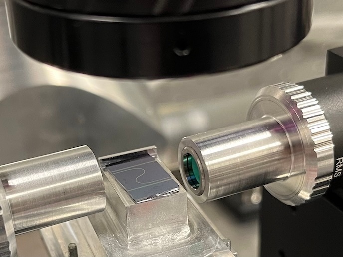
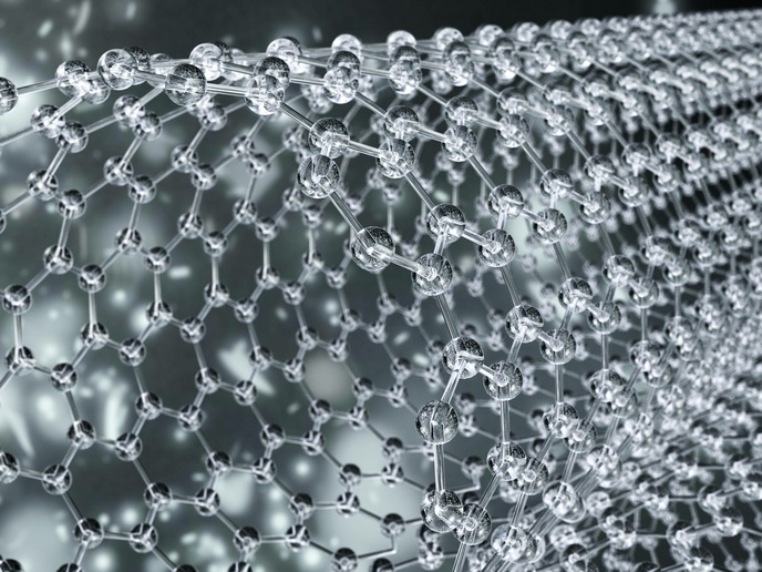
Electronic inks will be an essential link in the chain of events leading to the presence of electronic devices in everything we use, from clothes to books or even food packaging. Once fully developed, these inks are expected to remove most technical and design constraints while reducing production costs. They could just be the perfect support for new 2D materials, if it wasn’t for several difficulties associated to their preparation. Electronic inks typically consist of dispersed electronic materials, and, in the case of 2D materials, a long list of additives. But there is a catch: whilst preparation requires electronic materials of high purity, incorporating additives in the inks reduces the performance of these materials. The EU-supported 2D-INK project tackled this problem by developing a new approach to 2D material inks. As Prof. Aurelio Mateo, coordinator of the project on behalf of POLYMAT (the Institute for Polymer Materials of the University of the Basque Country), points out: “this is very challenging since 2D materials are like paper sheets than tend to pile up, and therefore cannot be turned into inks.” 2D-INK’s innovative inks, however, are not made of your average 2D materials. They boast the same structure as crumpled papers sheets, which prevents them from piling up and allows for mixing with liquids to form stable inks. “It wasn’t easy to get there,” says Prof. Mateo. “The whole project has been plagued by difficulties. To give you an example, once we had synthesised the new materials, we needed to ensure that they could actually be incorporated into the inks. As there are no available techniques to establish their structure, such techniques had to be developed in parallel to the synthesis process. Likewise, being able to produce an ink does not mean that it is going to have the properties you look for.” The consortium successfully overcame these difficulties thanks to joint efforts from different research groups with expertise in different fields of chemistry and physics. As Prof. Mateo willingly admits, doing it on his own would have been an impossible task. From synthesis to commercialisation The 2D-INK team already have explored several potential applications besides the fabrication of electronic devices, such as the modification of electrodes for electrocatalysis, or even energy storage applications. Such applications could emerge from further collaboration with Graphenea, a company that actively contributed to the formulation and characterisation of inks on the project’s novel 2D materials. As Prof. Mateo points out: “there is a high interest for 2D materials dispersed in liquid phases, as they are expected to lower the cost of fabrication of devices and products that incorporate the properties of 2D materials.” Graphenea has recently been split into two separate divisions, and one of them focuses on 2D materials dispersed in liquids. There are no plans for commercialisation yet, as several fundamental questions related to the performance of the new inks still need to be answered. However, Prof. Mateo is confident that, once these questions have been answered, it will be possible to start looking for the right cost/performance balance in order to make a product.