New plasma-based techniques for fabricating tomorrow’s high-performance electronics

While exceptional TMD properties have been demonstrated on mechanically exfoliated flakes, wide-ranging integration of these materials into complex devices remains extremely demanding. “Due to the extreme sensitivity and fragility of 2D crystals in comparison to classical bulk materials, all processing technologies used in semiconductor fabs have to be re-examined,” says Stefan De Gendt, main supervisor of the EU-funded PULSE2D project. “We developed plasma-based technology to clean, functionalise and etch TMD materials with atomic-scale precision.” This research was undertaken with the support of the Marie Skłodowska-Curie programme.
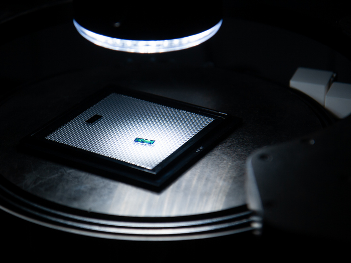
Plasma processing of TMD materials on full wafers
Individual Marie Skłodowska-Curie fellow Daniil Marinov began by gaining insight into the fundamental mechanisms of plasma-TMD interactions. He demonstrated that even in the absence of applied bias voltage, low-energy (under 10 eV) plasma ions are able to damage 2D layers beyond repair. “This means that for low-damage processes such as cleaning or functionalisation, ion bombardment should be fully excluded,” explains Marinov. “That’s why the application of a remote plasma source has been thoroughly investigated.” Together with project coordinator Interuniversity Microelectronics Centre (IMEC), the fellow demonstrated that polymer residues are fully eliminated by the remote H2 plasma, resulting in only a minor modification to the material properties. “None of the existing cleaning technologies are able to fully eliminate polymer residues without damaging 2D layers,” notes Marinov. Using ab initio simulations, they investigated the mechanisms of plasma-surface interactions. To reduce contact resistance in TMD-based field-effect transistors, the research team successfully applied remote hydrogen plasma in combination with molecular doping. “Plasma cleaning can reduce contact resistance, which is of primary importance because contacts limit the performance of ultra-scaled TMD devices.” Marinov also focused on applying the atomic layer etching (ALE) technique for wafer-scale integration of TMDs. “Selective etching of gate dielectrics is a critical step for contacting the TMD channel in field-effect transistors,” he elaborates. Marinov and the IMEC team examined ALE of high-k dielectric layers in BCl3/Cl2 chemistry. Findings show that by using the ALE process, gate dielectric materials can be removed selectively to silicon dioxide deposited at the TMD high-k interface. “For the first time, this allows formation of top contacts to 2D layers in a fab-compatible manner.”
Enhancing atomic layer deposition (ALD) nucleation
Improving film closure during atomic layer deposition of gate dielectrics on molybdenum disulfide, MoS2, was another aim of the project. “We showed that remote hydrogen plasma pre-treatment combined with molecular doping with Cl2 and carbonyl sulfide can be used to improve ALD nucleation on a TMD surface,” continues Marinov. “However, the improved nucleation comes at the expense of material damage.” To tackle this, an alternative ALD process with extended exposure of the TMD surface to precursor molecules was proposed. “The plasma processes developed during PULSE2D and the acquired fundamental understanding of plasma-surface interactions with 2D materials will be applied in producing new devices based on such materials for logic, memory and optoelectronic applications,” concludes Marinov.