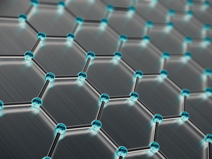
Advancing graphene device fabrication in Europe

An experimental pilot line is advancing European research efforts to create commercially viable graphene devices. Two multi-project wafer (MPW) runs for electronic and optoelectronic devices based on graphene and related 2D materials were recently completed on the pilot line. The results were presented in a recent study(opens in new window) supported by the EU-funded 2D-EPL and 2D-PL(opens in new window) projects. Graphene was first identified as a viable electronic material in 2004. However, 20 years later and despite significant efforts made towards large-scale manufacturing technologies, the semiconductor industry has not yet produced commercially viable graphene devices. The experimental pilot line for electronic and optoelectronic devices created under the 2D-EPL project was the result of EU efforts to support research in this direction. Building on this work, the project’s successor 2D-PL is working to further strengthen the European ecosystem by helping to mature semiconductor technologies and enhancing insight to aid industrial uptake. The two MPW runs reported on in the study were the first and third runs, completed at the end of 2022 and 2023. MPW run 1 was intended mainly for graphene-based sensors, in particular chemical and biosensors, and run 3 for graphene electronics.
Preparing for the MPW runs
The runs were preceded by an application phase, during which 60 applications from potential customers around the world were received for device designs, including electronic devices, bio and terahertz sensors, and photodetectors. Potential customers were provided with specification sheets with expected performance parameters for graphene devices, such as mobility, charge neutrality point, sheet resistance and contact resistivity. Another parameter measured was uniformity across the wafer, a key parameter for industrial processes. “If the target values were reached and the optical microscopy analysis showed an acceptable quality regarding the lift-off and etching, we considered the wafer ready for delivery,” report the study authors. A flexible process design kit with information on the available materials, fabrication methods and design rules was provided to potential customers. “After the application phase, the submitted chip designs were discussed individually with each customer. Then, all the customers’ dies were combined into a common mask design, and the required lithography masks were ordered. The mask also contained test dies with reference devices spread evenly across the wafer, in addition to the customer dies, to monitor process quality on every wafer of the run.” During the two MPW runs’ fabrication periods (in 2022 and 2023), over 75 wafers were processed. Raman spectroscopy – one of the methods used to monitor and inspect the different fabrication steps – was performed on the wafers after the graphene transfer and fabrication. Using this method, the research team “confirmed minimal structural changes in the graphene caused by the fabrication process,” according to the study. Furthermore, “electrical measurements of two different device types verified the device specifications defined in the process design kit.” “The results of the report indicate that the 2D-EPL platform is a promising one for prototyping graphene devices, for individual small customers as well as for larger industry,” reports a news item(opens in new window) posted on ‘Graphene-info’. The 2D-EPL (Graphene Flagship 2D Experimental Pilot Line) project ended in 2024. 2D-PL (2D-Pilot Line) ends in 2028. For more information, please see: 2D-EPL project 2D-PL project website(opens in new window)