Graphene microprocessor substrate accelerates electronic devices
Carbon exists in several physical forms, the most familiar being diamond and graphite (pencil lead). An additional structure called graphene(opens in new window) was discovered in 2004. Graphene is a single sheet of carbon, one atom thick, that can also form tubes. The material has extraordinary strength, electrical conductivity, and other properties. One of the many newly discovered uses for graphene is as microprocessor ‘interconnects’(opens in new window). These function as the internal wires of a chip, connecting its various micro-components. Current interconnects are made from copper, but graphene is a more efficient conductor. For this application to be feasible, graphene must be made compatible with existing industrial semiconductor tools and processes. This will involve integrating graphene into standard semiconductor substrates. However, semiconductor factories have very demanding purity requirements which, so far, have been proven difficult to meet. The EU-funded G4SEMI(opens in new window) project developed a solution that meets factory requirements, and offers graphene on a substrate that can be easily integrated into existing processes. The result is a new technology called graphene on wafer. The team demonstrated its suitability and scaled up its manufacture.
From prototype to pre-production stage
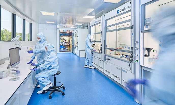
G4SEMI, as a phase-2 project, builds on the chemical vapour deposition (CVD) synthesis transfer technology developed in the EU funded Graphene Flagship project(opens in new window). This earlier project worked with potential customers to understand their needs and limitations. With that input, G4SEMI moved the graphene-on-wafer technology from a prototype to pre-production stage for the commercial semiconductor industry. “With CVD,” explains Jesus de la Fuente, G4SEMI coordinator, “we can deposit a high quality graphene layer on top of a special catalyst in a CVD reactor.” Catalysts accelerate chemical reactions. The first step in the deposition process involves preparing a copper-based catalyst, which creates a high quality graphene layer in the CVD reactor. The next step is growing a graphene layer on the catalyst. This involves putting the catalyst into the reactor under perfect temperature and pressure conditions. Any carbon gas can be the carbon source.
New transfer process and demonstrations
Customers need the graphene on a specific wafer, so it can be used in existing factories. “To achieve that,” continues de la Fuente, “we have developed a transfer process where we take the graphene layer from the substrate and move it to the carrier wafer.” The customer can insert this wafer into their standard manufacturing processes. The team demonstrated effective use of the new methods in CMOS (complementary metal-oxide semiconductor) factories that represent the vast bulk of the market. A key element was upscaling production of the wafers at the 200 mm scale that industry needs. Following the project’s success, the team has concluded a supply agreement with key industrial partners. This will involve increasing production capacity by 25 times. Using graphene for interconnects removes a key bottleneck in microprocessor speed. The technology will be applied to the manufacture of advanced medical biosensors with vastly improved sensitivity. It will also be applied to optical switches able to move 100 times more data than the existing optical fibres, and chips with higher memory densities.


