Increasing memory chip capacity using nanocrystals and long-chain molecules
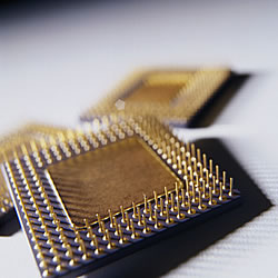
The EU-funded project SANEME has developed several techniques of great value for the manufacturing of hybrid microchips, combining traditional silicon-based fabrication with new nanotechnology. The main achievements are in the creation of nanogaps - very narrow (about 5nm) spaces between the metal electrodes in an integrated circuit - and the modelling and study of the electrical behaviour of molecules and nanocrystals. The fabrication of nanogaps between electrodes is important for the attachment of molecules to silicon chips. The project has developed two techniques for doing this. One, known as shadow evaporation, involves evaporating gold atoms at an angle to the layers of gold on the silicon wafer. The ‘shadow’ cast by the edge of one layer causes a gap of controllable size (between 2 and 6nm) to be formed. The second method involves the selective etching of a gap of around 5nm between silicon electrodes on a wafer, with the space being tailored to the size of molecule to be added. In both manufacturing techniques the molecules (in particular, molecules with thiol end-groups) are then added by self-assembly to form nanoscale electronic circuits. The electrical characteristics of these molecules, or nanocrystals, and their suitability for use in nanoelectronic devices, was then investigated as another part of the project. By practical experiment (using scanning tunnel spectroscopy) the properties of the molecules were found to depend strongly on the doping of the silicon base. Computer modelling was also used to find out what kind of properties are needed to work usefully in integrated circuits. Applications include memory chips, where the nanocrystals can be used for refresh of DRAM or TSRAM random access memory.