

Advanced thermal processing of semiconductor materials
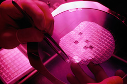
Cubic SiC (3C-SiC) is particularly attractive for Si-based devices as it exhibits the highest electron mobility of all known SiC polytypes. When (3C-SiC) is carefully grown, it is free of defects that are unavoidably present in other polytypes. However, this material is not yet commercially available in bulk single crystal substrates of acceptably good quality and large size. The FLASiC project consortium combined their skills and expertise to optimise the heteroepitaxial growth of a thin seed layer of cubic SiC on single crystal Si wafers for microelectronics applications. The research focused on defects due to the large lattice mismatch between the two materials, combined with the need to limit the growth temperature below the Si melting point. The main defects of high density reported are dislocations, stacking faults, micro-twins and cavities. Although, some of them are annihilated during subsequent growth, the remaining defects at the uppermost part of the SiC film are responsible for poor electrical characteristics of devices formed subsequently. The high defect density combined with wafer bending caused by thermal stress accumulation during the annealing cycles results in strained crystalline layers of poor quality, precluding device fabrication until now. Researchers at the CNRS-CRHEA developed a technique called "checker-board" carbonisation to minimise the undulating of the substrate. It balances a compressive (interfacial) stress by a tensile one to achieve the flatness required. The thermal processing of advanced semiconductor structures by an intense pulse of light with duration of a few milliseconds can thus be carried out in a systematic and well-controllable way. The main advantage of the process is that the area size can be adapted to the desired size opening up promising device and material fabrication possibilities.