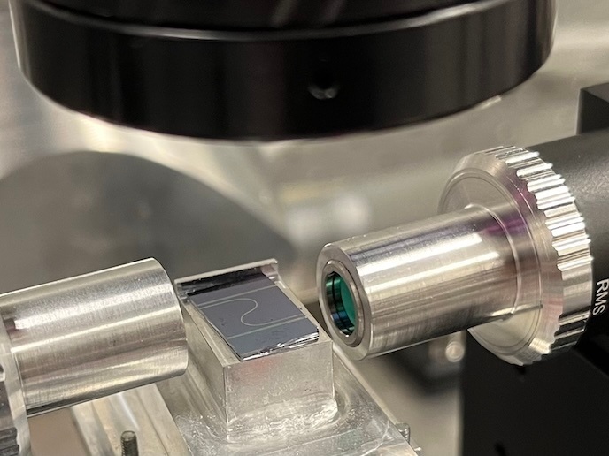
Optical nano-probe for spectroscopy and imaging
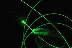
Due to the offered advantages such as easy processing, low cost and flexibility organic semiconductor devices like Light-Emitting Diodes (OLED), Thin-Film Transistors (OTFT) and Solar Cells (OSC) have become very popular. They may find applications ranging from flat panel displays to smart labels and identification tags. Aiming at the exploration of injector lasing in organic semiconductors at the solid state the OLI project focused on device structure, organic semiconductor growth and material synthesis. One of the key project results involves an innovative facility for ultra-fast spectroscopy and photolithography at the nanoscale. This novelty involves a unique combination of single and multiphoton femtosecond excitation with a laser scanning confocal microscope and photon counting streak camera detection. The novel coupling offers photoluminescence spectroscopy with in-plane spatial resolution of up to 120nm and temporal resolution of 2ps. With this set-up, 3D imaging capabilities blend with high sensitivity spectroscopic detection of time-resolved photoluminescence. Since imaging and spectroscopy are carried out on the same spatial position, the morphological characteristics are directly correlated to the spectroscopic properties. The advanced facility may be employed in the field of spectroscopic investigation and imaging of the active areas of molecular, electronic and optoelectronic devices. It constitutes a valuable tool for investigating nanoscale phenomena and contributes to the assessment of organic, hybrid and biological nanostructures and nanodevices.