Optimising chemical sensors
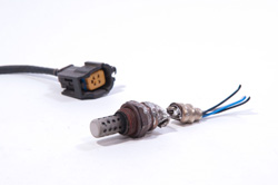
With the advent of nanotechnology, nanostructures have been widely employed in various types of sensors. Because of their small size, the nanostructures and materials have altered physical and chemical properties requiring tiny amounts of chemical vapour to change their electrical properties. As a result, they can detect very low concentrations of a given chemical. To understand the nanoscale phenomena that control nano-structured sensors and functionalised surfaces, the EU funded the project ‘Nanostructures for chemical sensors’ (Nanochemsens). The ultimate goal was to exploit such phenomena in order to develop the appropriate surface science tools and nanotechnological processes of future chemical sensors. As a first step, the research team developed suitable techniques for controlled fabrication of nano-structured sensors and investigated the sensor/molecule interactions on functionalised surfaces. They used titanium dioxide – a semiconductor which has long been used in surface science investigations and is an ideal candidate – to investigate the properties of nanostructures fabricated on functionalised surfaces. Tungsten oxide was also explored for construction of thin film sensors due to its high sensitivity towards various gases (Nox, H2S, NH3, O3). project partners succeeded in determining the voltage curves of a single platinum particle with a diameter of 8 nm, deposited on a clean titanium oxide surface. Additionally, various surface reactions were tested for the cross-sensitivity of oxide sensors to humidity. Finally, metal oxide/organic film blends were explored for their use as sensing layers for detection of volatile organic compounds (VOCs). implementation of the Nanochemsens surface science and nanotechnology approaches to sensor research and development (R&D) will likely lead to scientific and technological advances, and will reinforce competitiveness of European sensor companies.