Electro-optical technology enhances the global EU position
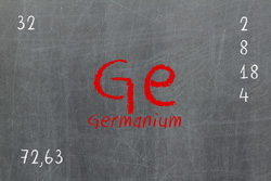
Crystalline (epitaxial) SiGe alloys are the subject of intense research and development in Asia and the United States. They are paving the way to novel photonics and electronics, including high-speed transistors and infrared (IR) detectors. In order for the EU to remain competitive in this growing field, scientists initiated the EU-funded project 'Photonic integration on silicon germanium' (PIOS). Investigators focused on a relatively new technique, multiple hydrogen annealing for heteroepitaxy (MHAH), which enables the production of very high-quality Ge layers integrated on a Si complementary metal-oxide semiconductor (CMOS) platform. They used the technique to grow SiGe multi-quantum well (MQW) structures. Literally small well-type structures produced by layers of materials, the 'wells' confine charge carrier (e.g. electron or hole) movement in a direction perpendicular to the layers. Quantum wells enable the control of energy conversion into light at desired wavelengths. When the control or modulation is via an external electric field (via the quantum-confined Stark effect (QCSE)), an electro-absorption modulator is created. PIOS exploited MHAH-grown SiGe MQW structures and the QCSE to produce highly responsive photodetectors and high-performance electro-absorption modulators. In addition, the selective area epitaxial growth (SEG) procedure enabled the growth of SiGe layers compatible with conventional Si CMOS processes. Scientists also used the epitaxy technique to grow Ge semiconductor nanocrystals in a conducting Si matrix, a major advantage to production in an insulator as has typically been the case in other studies. In addition, the team produced Si nanocrystals using low-cost, high-throughput laser ablation that could provide materials for a variety of opto-electronic devices and implemented them in a novel photodetector concept. PIOS techniques and devices are expected to have major impact on the European opto-electronics industry and its competitive position in a growing global market. In addition, novel devices such as inexpensive and very fast telecommunications, point-of-care spectroscopic diagnostic systems and machine vision for the automotive industry that exploit project outcomes will ensure that EU citizens share the wealth.