Pioneering micro-Transfer Printing achieves wide platform compatibility
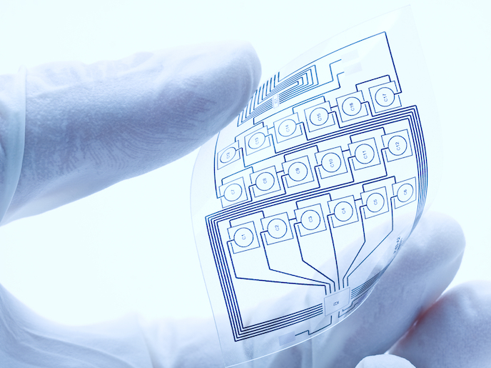
The evolution of smart systems relies on a combination of technological advances such as increased functionality and miniaturisation, which necessitates further integration of components. Ideally these inter-connected devices would be formed by precision placement on a substrate (platform), but this presents a number of challenges. The new technique of micro-Transfer-Printing (micro-TP) offers a way forward as it separates the essential materials or devices held on their native substrates and in a ‘pick and place’ manner transfers them onto a new substrate, with a very high degree of accuracy. These devices are only a few micrometres (one millionth of a metre) thick. The TOP HIT project was established to develop and validate the micro-TP technology using Photonic Integrated Circuits (PICs) on silicon substrates for the communication industry. This offered indicators of the technology’s value for system designers and low-cost manufacturing. The project also demonstrated the integration of very compact electronic circuits onto non-silicon substrates, overcoming previous barriers of incompatibility between different technological platforms. Achieving submicrometre integration Smart systems, by their very nature, integrate many different functionalities, for example sensing, actuation, modulation and signalling. But this presents a challenge for designers at it is predicated upon electrical, optical, thermal and mechanical considerations. Optical connections are particularly challenging as the waveguides need to be aligned to each other with submicrometre precision for the highest performance. By transferring extremely thin devices from a source wafer to a target wafer platform using micro-TP, the devices can be connected using metallic redistribution steps. As the method minimises the required spacing between components on the source substrate, compared to the target substrate, so it greatly increases the efficient use of the expensive source materials and devices. As project coordinator Mr Brian Corbett says, “The technique can be engineered to suit a wide variety of devices and works best with components that are less than 500 micrometres in lateral size – a regime where other methods struggle. The main requirement is that the receiving locations be locally flat which can be achieved using an adhesion layer of submicrometre thickness.” Efficient electronic subsystems offer a range of possibilities The technique especially holds out promise for data communications where high bandwidth and high density of interconnected components are requirements. Uptake is first expected in data centres and then in access networks (fibre to the home), allowing high-performance transceivers at low cost. Additionally, the technique’s ability to combine customised light sources, detectors and electronics in miniature subsystems opens the possibility for use in medical diagnostics (such as for endoscopic applications), environmental sensing and displays. Expanding on the possibilities for the consumer market Corbett says, “Having worked in photonics for many years I am aware of the power of lasers for information delivery, especially for the internet. However, until now the technology hasn’t had the same impact on consumer applications. Powerful photonics containing subsystems at consumer prices will change this.” So far TOP HIT’s demonstrations of the micro-TP technology have been undertaken with small volumes. Currently an open source pilot line for the integration of micro-TP -enabled smart systems in a semiconductor foundry manufacturing environment is underway through the microprince.eu (Microprince project) under the ECSEL programme(opens in new window). This will yield a number of individual applications for further development. Future work will also need to develop manufacturing standards with design rules (such as process design kits) on how to best interface with foundry technology.