Mass transfer via elastomeric stamps achieves industrial-scale fabrication of 3D integrated microelectronics
Integrated circuits or ‘chips’ replaced the discrete components and soldered joints of conventional electronics with many circuit elements on a semiconductor wafer. This facilitated ever greater functionality and higher performance, significantly smaller sizes and weights and lower energy consumption. It also slashed production and testing costs and waste. Photonics integrated circuits are doing the same for optical devices and optoelectronics. As performance demands continue to increase, achieving device scaling and cost reduction requires a new modus operandi. Heterogeneous integration unites dissimilar and separately manufactured components on a common platform in a so-called system-in-package. The EU-funded MICROPRINCE(opens in new window) project has established a foundry pilot line for heterogeneous integration based on one of the most promising techniques under development over the last 15 years. A diverse portfolio of demonstrators paves the way for innovators to expedite the production readiness of their groundbreaking devices in multidisciplinary fields.
A rubber stamp for almost any kind of ‘paper’
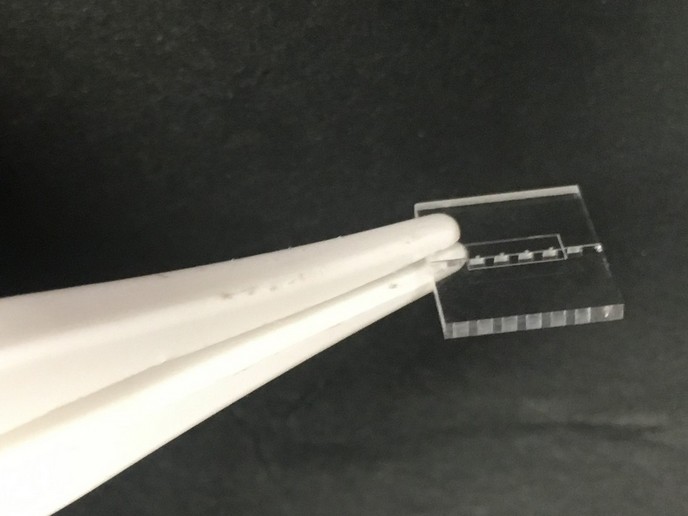
With increasing component and product complexity, the likelihood of failures increases, increasing scrap and costs and decreasing yield. Integrating multiple ‘chiplets’ or subsystems is more practical and economical than producing monolithic systems. One of the most promising approaches is micro transfer printing(opens in new window) (μTP), also called mass transfer. μTP uses an elastomeric stamp to move up to thousands of chiplets or wafer fabricated microscale devices at a time from one substrate to another, like ink in an inkpad is transferred to paper. Until now, the technique was used mostly in labs for scientific research.
Demonstrated flexibility for tomorrow’s high-tech applications
MICROPRINCE established a μTP pilot line in the X-FAB MEMS Foundry(opens in new window) clean room and rolled out four high-tech products. These were gallium arsenide Hall plates(opens in new window) for next-generation current sensors, human-eye-response filters for ambient light sensors, gallium nitride LEDs(opens in new window) for car ambient lighting modules and indium phosphide photodiodes in silicon photonic circuits(opens in new window). These products were used in functional demonstrators of ambient light sensors, car ambient lighting drivers/packages and integrated silicon photonic infrared spectrometers. According to Sebastian Wicht, MICROPRINCE coordinator and programme manager of transfer-printing at X-FAB MEMS Foundry, “in addition to µTP pilot line creation, generic process developments supported the excellent potential of µTP for 3D integration with high yield, throughput and alignment accuracy. We demonstrated printing or transfer yields of up to 99 %, with misalignments below 1.0 µm. Devices with sizes as small as 100 µm x 100 µm x 5 µm were effectively transferred and stacked on complementary metal oxide semiconductor target dies.”
Massively parallel packaging and superior performance with minimal waste
µTP enables the transfer of thousands of microdevices in a single step with excellent accuracy for very high throughput at comparably low cost. It surpasses state-of-the-art technologies in minimising package size and nearly eliminates the waste of expensive materials and elements. Wicht concludes: “MICROPRINCE has paved the way to industrial implementation of µTP for 3D and heterogeneous integration. It will support the development of innovative products with superior performance, smaller package sizes or even new functionalities in fields from industrial and consumer products to biomedicine.” Interested customers are encouraged to contact X-FAB MEMS Foundry to bring their ideas for new applications to the production realm.


