Taking printed electronics ideas all the way to market

Printed electronics play a vital role in the development of the Internet of things (IoT). Our homes, cars, and even our clothes and accessories are fitted with electronic devices such as circuits, sensors, displays and labels, all of which are produced using printed electronics. However, despite the innumerable possibilities of printed electronics applications, there’s a wide gap between a new concept and market entry. To speed up the development and manufacturing of functional nanomaterials and printed components, the EU-funded LEE-BED project is providing an open innovation test bed (OITB) to test printed electronic applications. “Through LEE-BED, we are joining forces with some of Europe’s most prominent research and development institutes and SMEs, to provide consultancy services and access to state-of-the-art facilities within printed electronics,” stated Zachary James Davis of LEE-BED project coordinator Danish Technological Institute in an article(opens in new window) posted on ‘Printed Electronics Now’. “The goal is to strengthen the European competitiveness through novel technologies.”
Test bed services and pilot lines
Through the OITB, the LEE-BED team provide a wide range of consulting services and access to different pilot lines. The process is divided into three phases. First, the idea is screened and evaluated. Services such as technical assessment, pre-safety assessment, economic assessment, life-cycle assessment, patent mapping and pilot project funding support help companies see how feasible their idea is. The second phase involves developing the idea from the design stage to prototype, or even further to pilot production. Companies have access to pilot lines that can produce functional nanomaterials and printed electronic components. In the third and final phase, a range of essential services involving intellectual property rights and patents, standardisation and safety, business planning and connections with potential investors help to bring the knowledge gained to market.
Current industrial end-user cases
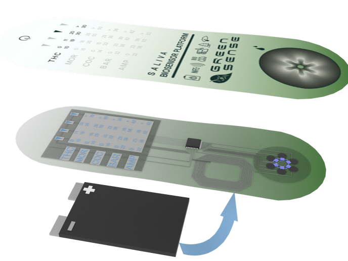
The project team is already working on four cases in the following application areas: autonomous structural monitoring systems, decorative intelligent surfaces, smart dashboards, and intelligent labels. “We are now working with four industrial end users, Swarovski AG working with wearables, MAIER working with automotive plastic parts, Grafietic working with labels and ACCIONA working with construction,” explained Davis. “In the fall, we will open our services to external companies and run 10 service packages free of charge in order to get LEE-BED started.” According to Davis, the LEE-BED (Innovation test bed for development and production of nanomaterials for lightweight embedded electronics) OITB has the potential to play an important role in the growth of printed electronics. “Printed electronics has been around for several decades, in products like membrane switches,” he remarked. “However, there are many new applications which will be enabled by printed electronics, such as IoT, eHealth, and smart packaging, just to name a few. For this to happen, new materials and process [sic] will be developed, thus there will be a large demand for LEE-BED services and pilot line access.” For more information, please see: LEE-BED project website(opens in new window)