Improved microscopy technique reveals previously hidden magnetic secrets of smart materials
Smart or functional materials, the latest revolution in the material science field, can adapt their physical or chemical properties depending on changes in their surroundings. They form the bedrock of modern society as they grace all our modern devices, from smartphones and computers to satellites and cars. Until now, electronic device makers have been piggybacking on the renowned Moore's Law for delivering successive generations of increasingly small, dense and more powerful chips. Silicon integrated circuits have been underpinning almost everything in our digital world. However, the performance of silicon-based devices will soon hit a wall. “New classes of functional materials are being eyed as a way to replace silicon when it will fail to deliver for increasingly small chips,” notes Magnus Nord, Associate Professor at the Department of Physics in the Norwegian University of Science and Technology. “Magnetic materials are a prominent class of materials that possess several smart abilities. Their magnetic response to an external magnetic field renders them suitable for use in various applications including data storage, communications and sensors. To design such devices from often complex magnetic materials, it is necessary to understand how they work at the nanoscale. Once at this scale, the fascinating world of quantum mechanics takes a bigger hold,” explains Nord.
Clearing the hurdles to nanoscale imaging of functional properties
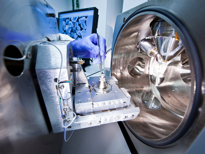
Lack of proper experimental techniques for studying the intriguing magnetic properties at the nanoscale is preventing magnetic materials from making a bigger impact. In the context of MAGIMOX, a project undertaken with the support of the Marie Skłodowska-Curie Actions programme, while working at University of Antwerp, Nord worked on extending the capabilities of scanning transmission electron microscopy(opens in new window) (STEM) into previously untapped segments. “STEM is a powerful imaging technique, which can painstakingly image single atomic columns in a material. However, the technique does not lend itself to studying the functional properties of materials but rather their structure,” notes Nord. “Although pixelated STEM detectors(opens in new window) have enabled us to directly image magnetic fields in materials, they have still much room for improvement, most notably in their ability to work practically on most STEM instruments and across a range of materials.” The project team optimised several data processing algorithms for studying magnetic phase transitions in thin films of perovskite oxides, a special class of materials that feature a great variety of functional properties. All code updates were included in pyxem(opens in new window), an open-source Python software library. A great deal of work was also geared towards STEM calibration and alignment. Alignment optimisation is deemed highly necessary as the major lens is turned off during operation, greatly affecting the electron optics of the microscopy system. Apart from investigating the magnetic properties of thin-film perovskite oxide La0.7Sr0.3MnO3 researchers made great progress in the study of structural phase transitions in another class of readily available functional oxide materials that were heated. Improved data processing algorithms enabled the study of structural phase transitions on a wider range of STEM instruments and over much larger fields of view. Smart materials might have just started extending out of the realms of the laboratory but have a variety of potential applications outside their core area of electronics such as in actuators, aircraft structures and drug delivery systems. Uncovering how they work at the nanoscale could spark innovation in all sorts of such applications.