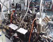
Thin film fabrication
Molecular beam epitaxy is a standard technique for depositing thin layers of semiconductor materials onto a suitable substrate. Gallium nitride and related nitrides, derived from an advanced nitrogen source, have been grown on silicon and sapphire to form semiconductor materials with excellent properties. The source for the nitrides is an electron cyclotron resonance plasma source operating at 2.45 GHz. An ammonia injector operated at temperatures below 600°C produces good growth rates of good quality material. The injector can work at higher temperatures for cleaning purposes. Optimal uniformity, doping and alloy composition of the layers can be achieved with careful source positioning. The properties of the layers produced show that they are of a quality suitable for devices such as field effect transistors and light emitting diodes. This is a cost-effective and environmentally friendly method, requiring less ammonia than other processes. Future developments will aim to improve the quality still further and explore the possibilities of new materials and substrates. Ultraviolet detection is an application of particular interest.


