Contributing to the production of nitride-based electronic devices
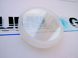
Research on the new nitride-based materials showed that they can bring significant breakthroughs in the fields of electronics and opto-electronics. For instance, GaN-based semiconductors may find widespread applications ranging from displays and data storage to medical diagnosis and radars. European research activities in this area are lagging behind compared to other regions and, as a result, Asian and US industries have already taken stronger positions in the opto-electronics market. In order to bridge the present gap and increase employment opportunities for European industry, the EURONIM project focused on the creation of industrial sources of nitride epitaxial wafers. High quality GaN epitaxial wafers were among the various industrial products developed during the course of the project. After Si, GaN is considered one of the most important semiconductor materials used for the next generation high frequency and high power transistors capable of operating at very high temperatures. Apart from its exceptional properties, GaN is also environmentally friendlier and less toxic than other substances, minimising health hazards. Within EURONIM, standard GaN/sapphire templates were produced allowing the fabrication of templates with low dislocation density. These pseudo-substrates can be used for the growth of nitride based device structures, such as UV detectors or transistors. Employing a special technique called Epitaxial Lateral Overgrowth (ELO) GaN/sapphire pseudo-substrates with very low defect density have also been developed. Moreover, using the Hydride Vapor Phase Epitaxy (HVPE) method on ELO quality GaN/sapphire, thick GaN layers were grown. With the aid of a laser lift-off or other technologies the sapphire was separated, resulting in free-standing GaN that can be used for the fabrication of laser diodes. Despite some minor improvements required in the production process, the potential of the new GaN structures is significant. It is expected that such efforts will promote the production of substrates for the growth of nitrides in Europe. Furthermore, project results can also benefit European nitride foundries by the development of new, innovative and high-added value electronic and opto-electronic devices.


