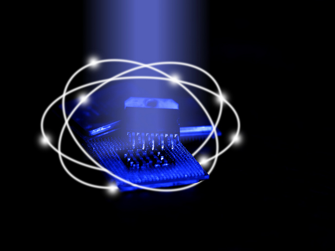
SEM-on-a-chip at a fraction of the cost
Commercial SEMs are large and expensive instruments. While scientific principles existed enabling the scaling down of device size and the resulting minimisation of energy requirements and image aberrations, only with recent advances in nano-machining technology has the practical realisation of such devices become possible. European researchers supported by funding for the ambitious ‘Ultra-bright nanoscale SEM-on-a-chip’ (Monarch) project set out to do just that, namely to develop the world’s first sub-miniature SEM-on-a-chip. Monarch produced a device only 5 micrometres long (a human hair has a width of about 50 micrometres) operating at lower voltages and with atomic resolution an order of magnitude higher than current state-of-the-art SEMs at a fraction of the cost. The ability to produce ultra-low energy, ultra-high power and ultra-pure electron beams enables for the first time rapid scanning of a surface layer and elemental identification at atomic resolution. Dramatic implications of the new device impact important fields including gene sequencing, ultra-high density data storage and focused ion beam milling, to name just a few. Of crucial importance, nano-patterning of electronic devices using electron beams may now be commercially possible. The ambitious Monarch project delivered the first sub-microscopic SEM capable of being integrated on a chip and having an order of magnitude higher resolution at a fraction of the cost of state-of-the-art SEMs. The device is positioned to revolutionise electron beam technology and the nanosciences with far-reaching and tremendous effects on European competitiveness.