Taking the stress out of nanomaterials design
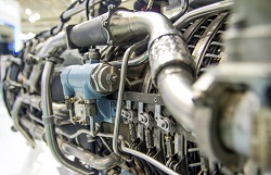
All materials contain residual stresses - intrinsic stresses that remain within a material, usually arising from the way they have been manufactured. ‘Component performance can be remarkably improved if residual stresses are properly controlled and assessed and that is what ISTRESS has investigated’ says Marco Sebastiani, a Materials Scientist from Roma Tre University Italy and ISTRESS project coordinator. The three year EU-funded project, completed in 2016, has developed methods to analyse and modify these stresses at the nano-scale. ‘Controlling residual stress is a very important factor to be able to improve reliability and strength of nanomaterials,’ explains Sebastiani. Residual stress affects mechanical properties, such as strength, adhesion, friction and wear. This is particularly the case with nanomaterials such as the thin films used in mobile phone components and medical prosthetic materials used for replacement knees and hips. ‘Residual stress distribution across interfaces can strongly affect layered materials and for example, can lead to premature failure of thermal barrier coatings and superalloys in aircraft engines,’ says Sebastiani. ‘The ability to design, measure and control residual stress with sub-micron scale resolution can have a dramatic effect of the performance of such components,’ he adds. The ISTRESS consortium set out to improve nano-scale residual stress analysis. Established techniques are expensive and therefore often not available to industry. ISTRESS has tried to fill this gap with a novel high-resolution method to measure residual stress with sub-micrometer spatial resolution and all at a reasonable cost. They developed a three-step method using a focused ion beam (FIB) to remove nanoscale amounts of a material being tested. Using a Scanning Electron Microscope (SEM) and Digital Image Correlation (DIC) - an image-analysis method that tracks image changes - the residual stress is measured by detecting the changes in shape (known as relaxation) associated with material removal. The method (FIB-SEM-DIC) is fully automated so complete measurement can be taken in one hour, using microscopes designed and manufactured by the Czech company TESCAN (a full ISTRESS partner). The team communicated with two industry standardisation organisations, the European Committee for Standardisation (CEN) and The Versailles Project on Advanced Materials and Standards (VAMAS), to establish a standardised methodology that was tested on industrially relevant reference samples. The method has already been used by two industry partners to optimise the development of new materials. German company Bosch developed a novel multilayer coating to be used on the valves of diesel engine injection systems. By tuning the residual stress profiles, they achieved a remarkable increase in the wear resistance of the components, with no increase in production cost. French multinational company Thales has tuned and improved the stress distributions in an innovative micro-electromechanical system they have developed for application in avionics, gaining performance improvement at no extra cost. For industry, this new method creates access to previously uneconomical design optimisation methods. ‘Acquisition of a FIB microscope is difficult for SMEs, but we have reached the required level of automation that allows companies to access this method by simply renting a day of FIB time’ says Sebastiani. ‘Several European companies outside the ISTRESS consortium are already using this new method to develop their own products.’