Repurposing a standard technique for nanoscale optics
Cathodoluminescence (CL) is a physical phenomenon first observed in the 1960s whereby light is emitted by a material when hit by an electron beam. Historically, CL was used in cathode ray tube televisions to generate images and by geologists to characterise minerals.
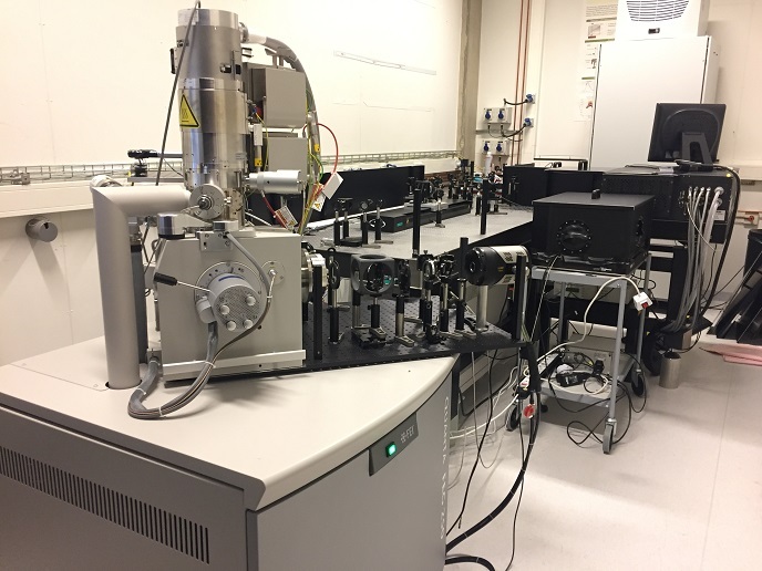
A novel CL-based electron microscope
Scientists from the European Research Council (ERC)-funded SCEON project combined the properties of CL spectroscopy and electron microscopy imaging into a novel CL system(opens in new window). In CL spectroscopy the light emitted by structures when they interact with the electrons is collected and analysed, offering functional optical information. “Our goal was to combine the advantages of electron microscope and optical imaging into a novel system, unique in the world,″ explains ERC grantee and principal investigator, Albert Polman. CL provides information on the interaction of light and matter and, because it uses electrons, its resolution is at the nanometre scale. The SCEON CL system works by collecting the photons emitted from the sample bombarded with electrons through a parabolic mirror. This boosts the light-collection efficiency of nanostructures and also enables measurements on low light-emitting samples like metals. At the same time, the SCEON technology has many practical applications in geology, semiconductor metrology and photovoltaic materials fabrication, improving the performance of light-emitting devices and solar cells. Manipulation of single photon sources using the CL system will enable further development of quantum information technology. Furthermore, the SCEON CL system also enables the study of how the emitted light behaves over time at the nanoscale. This provides scientists with the opportunity to study the underlying physics phenomena at this small-length scale and answer fundamental questions related to the interaction of electrons with nanostructures. The use of electron pulses gives the SCEON CL system the capacity to provide new insight into the dynamics of electron and light excitation as the device allows temporal resolution. A wide range of interesting results have come from the SCEON CL microscope studies including the study of light emission in different nanostructures. Researchers have also been able to determine the emission efficiency at very high spatial resolution of semiconductors used in solar cells, and to study the interactions of ultrafast laser and electron pulses mediated by metallic nanostructures.
Future prospects for the CL microscope
The CL microscopes were developed in collaboration with AMOLF, Thermo Fisher and Delmic, which brought the first commercial version of the instrument onto the market in 2014. The CL microscope has also been awarded the Materials Research Society ‘Innovation and Materials Characterization Award’(opens in new window). “We received the SCEON ERC Proof of Concept grant to develop a commercial, table-top version of our new microscope that can potentially be used by a broad range of users,″ emphasises Polman. Since the first characterisation of the CL physical phenomenon, researchers have advanced CL imaging spectroscopy for more scientific purposes. “Our system offers the capacity to study essentially every metal, semiconductor, dielectric material or nanostructure and physically see, very precisely in space, how light resonates in these materials, the direction it is emitted and the duration of these interactions,″ continues Polman. Understanding how high-velocity electrons interact with nanostructures will help the design and implementation of cheaper and more efficient photovoltaics, miniature opto-electronic circuits and light-emitting diodes.