Improvements for nano imprint lithography
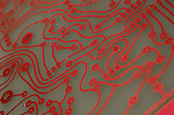
A few years ago the major obstacle in developing nano-structures has been the fact that there was no manufacturing technology able to provide high-throughput and low production cost. Nano Imprint Lithography (NIL) proved to be an effective solution to this problem. According to NIL, a mold of a specific pattern is stamped on a polymer surface. The imprint is then heated so that the residue of the polymer in the compressed area can be removed. Finally, the metallization of the imprint takes place and the desired nanostructure is created and lifted-off. CHANIL project focuses on NIL, and particularly on approaches that can improve two points crucial for the completion of NIL: the stamp's removal and the lift-off of the structure. A dry chemistry method was developed within the project for the anti-stick treatment of lithography stamps made of either Nickel or Silicon. The stamp - polymer interface has perfect anti-sticking properties after the treatment, ensuring that no parts of the polymer will stick on the stamp altering the structure’s shape even after multiple stamps. Regarding the lift off phase a new technique has been introduced. This technique relies on the adjustment of temperature and time in order to optimize the flow of the residual's layer as well as the use of a diluted solvent for its final removal. These two innovations not only make NIL more effective but also, and perhaps most importantly, they make possible the production of even smaller nano-structures.