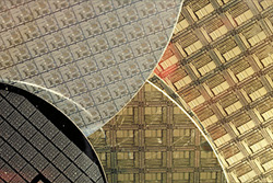
Looking into the future of nanofabrication
With the advent of the Information Age, semiconductor devices have become faster with larger capacities in smaller dimensions. For further improvements, tighter packing of ICs with finer line widths has become essential. Towards this aim, a very promising lithography technology is the VUV, which has not until recently been developed to its full potential. In 1999, the International Technology Roadmap for Semiconductors (ITRS) has suggested VUV lithography (157nm exposure wavelength) for manufacture of the 100nm and 70nm technology node. A key problem involved was the very short time frame from the commercialisation of 157nm step and scan systems to the insertion of the lithography technology into production. Urged by this the UV2Litho project focused on accelerating process development for the introduction of VUV lithography technology in production lines. Therefore, the manufacturability of resist processes was extensively investigated which allowed demonstrations of 157nm resist solutions for the 70nm node. Additionally, information on the printing performance of early 157nm reticles for the mask making industry was also revealed. Nevertheless, an alternative technology, namely the 193nm immersion lithography, has been rapidly developed, having the potential to realise sub-70nm groundrules. On the other hand, the 157nm infrastructure industry could not meet the very stringent requirements for the related technology components. For this reason the market interest shifted from 157nm to 193nm immersion lithography. Despite that, the feasibility of the 193nm immersion technology has not been yet fully proven in terms of its production value. Thereby, in case of failure, 157nm lithography is expected to supersede as reflected by the current ITRS roadmap. The UV2Litho project has set the base for the exploitation of the VUV lithography. For more information click at the project site: http://www.imec.be/uv2litho/(opens in new window)


