Large-scale analysis of nanostructures
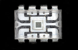
Proximity sensors are probes able to detect the presence of nearby objects without touching them. Scanning proximity probe (SPP) microscopes, among them atomic force microscopes (AFMs), measure local properties such as height or optical absorption using a probe tip in close proximity to the sample. The probe itself is a cantilever, a very thin needle-type structure. When passed over the surface of a sample, SPPs enable molecular-level characterisation and manipulation of particular importance to the field of nanotechnology. To date, SPP nanotools consist of only a few probes with limited readout and slow processing rates primarily used for research. Development of massive parallel probe arrays and the use of ‘smart’ materials could dramatically enhance speed, surface resolution and manipulator control, leading to development of a whole new class of nanotools for industry. European researchers sought to produce parallel arrays of cantilever sensors using piezoresistive (PR) materials. PR materials are one of many classes of smart materials. They respond to mechanical stress with changes in resistance to electrical current flow. With EU-funding of the ‘Tools and technologies for the analysis and synthesis of nanostructures’ (Tasnano) project, scientists sought to build the PR technology into a generic, parallel-module nano-electromechanical system (PM-NEMS) that could be functionalised to produce application-specific NEMS-chip packages (AS-NEMS). Tasnano concepts should enable functionalised and tailor-made industrial-scale analysis, control and manipulation of nanostructures. They could have impact on high-speed data analysis, new product synthesis and a whole host of applications yet to be discovered, driving rapid development of nanotechnology processes and their commercial exploitation.