New techniques for better solar panels
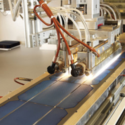
The major challenge for solar panel manufacture today is creating a 50-micrometre–thick silicon layer, the theoretical peak for energy conversion efficiency. Funded by the EU, the 'Silicon substrates from an integrated automated process' (SUGAR)(opens in new window) project aimed to address this problem by developing techniques for producing such thin silicon layers. These techniques were to be carried through to a manufacturing process to create solar cells equipped with the new wafers. Researchers tested a range of stress-inducing coatings that caused silicon wafers of approximately 50 micrometres to crack off of the silicon substrate when heated. They tested metal, glass and polymer pastes before settling on an epoxy that performed as desired at relatively low temperatures (150 degrees Celsius). The second part of the project focused on using such thin layers to create solar panels. Researchers developed a new technique that involved bonding the silicon layer directly to glass plates, making further handling much easier. Much attention was given to developing and testing new manufacturing processes to incorporate these techniques. Finally, SUGAR produced a proof-of-concept prototype solar cell module using these new processes. The research conducted during SUGAR has provided a new, cheaper way to produce silicon wafers, leading to more efficient solar panels with reduced silicon usage.