

Towards extreme ultra violet lithography
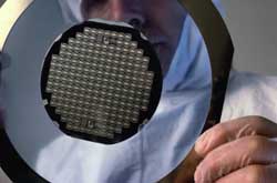
Moore's law, apart from the progress made in the semiconductor field, also clearly shows the intensity of competition between industries. This rate of progress will eventually slow down due to anticipated physical and engineering limitations. Additionally, the need arises for huge investments. Integrated circuit manufacturers specifically, in order to establish a successful business, need continuous product and process development. A consortium of European industries has undertaken a research and development program on the evaluation of extreme ultra violet lithography. Lithography, in the context of integrated circuits, is an elaborate printing process used to put patterns onto silicon wafers. Though similar in principle to the usual photolithographic process, building state of the art chips places severe restrictions and requires different procedures. The current volume manufacturing method is optical lithography, characterised as such from the use of visible or ultra violet light. The shorter the wavelengths of light used, the smaller the features that can be print on the wafer. Starting from blue at 436 nanometers, wavelengths have gone down to deep ultra violet at 248 nanometers. The current project addresses the problems associated with the use of extreme ultra violet light and anticipates commercialising this type of lithography by 2008. The light used will be from 70 nanometers and below. By advancing fabrication technologies, integrated circuits manufacturers will be able to develop new products and remain competitive in the global market. Moreover project partners, in order to ensure viable system concepts, design equipment in modules so that as technology requirements increase, industries can upgrade their systems, while keeping the original capital investment intact.