Minimising defects in plastic electronics
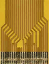
Electrically conductive polymers, whether organic or carbon-based, are physically flexible and can be produced with low-cost printing, coating and spraying technologies. Products such as organic light-emitting diode (OLED) displays provide significant performance and energy benefits compared to liquid crystal and plasma displays. Although plastic electronics offer exciting benefits compared to conventional inorganic semiconductor materials, the immaturity of production techniques leads to defects and inhibits their mass production. Scientists are optimising the application of real-time digital radiography for volumetric detection of defects with the EU-funded project 'Development of an automated digital radiography system for the inspection of plastic electronics' (PLASTRONICSSPEC)(opens in new window) . The target application is inspection of OLED screen panels. Scientists are employing simultaneous multi-mode signal processing to optimise the use of X-ray photons for better minimum detectable defect depth and spatial resolution. The team obtained good and defective OLEDs and other plastic electronics samples and tested them with general-purpose X-ray radiography equipment. Such inspection was carried out on OLED panels as a reference for the system to be eventually developed within the project. It also helped define the new system's requirements, including X-ray source, detector, setup and cabinet as well as supply and feeding of components to the inspection system. Experiments have aided in the design process as well, with scientists evaluating various setups and key radiographic parameters for maximum spatial resolution. Significant attention has been given to safety aspects of the enclosure system. OLED panels and plastic electronics with controlled defects were manufactured to be used in future testing of the sensitivity of the PLASTRONICSSPEC inspection system. Finally, the partners have prepared dissemination materials and hosted an exhibition stand at The UK Plastic Electronics Show 2012. PLASTRONICSSPEC technology will have major impact on the numerous small- and medium-sized enterprises working in the field of plastic electronics. Non-destructive testing of pieces on the production line will minimise defects, material waste and production costs for enhanced consumer confidence, increased profitability and an impressive return on investment. Watch the project’s video(opens in new window) here.