New models for minimising probe tip burn
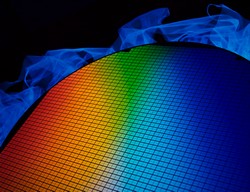
As devices and thus test probe tips shrink in size, the current carrying capability (CCC) of the probe is also reduced. At the same time, the maximum current required to test some components is increasing. Taken together, the risk of current-related probe tip damage or burn is increasing and that, in turn, can damage the wafer itself. Scientists successfully developed models of CCC phenomena to enable better probe designs for high-power wafer tests with EU funding of the project PROBE-BURN (Probe burn phenomena: Predictive modeling and characterization for high power wafer test applications). The CCC is critical to probe cards and mainly depends on the probe tip diameter, ambient temperature, thermo-physical material properties, the duration of the applied current and the contact resistance at the probe tip-bond interface. Scientists successfully developed a numerical method that can compute temperature distribution along a probe body. Experimental and numerical results were in excellent agreement, confirming the validity of the numerical methods to determine CCC. The team also developed models that help optimise probe designs and predict CCC limits accurately before damaging the wafer. Furthermore, new simulations were developed to analyse heat transfer between the heated probe and its surrounding environment. Experiments with spring probes that were conducted in laminar air flow and without air flow were in good agreement with numerical results. Probe burns are an increasingly prevalent problem associated with wafer tests. Novel tools to both design and monitor probe tips during wafer tests should significantly reduce the impact of this pressing problem. This is also slated to result in significant savings for the semiconductor industry in terms of money, time and resources.