

Delivering miniaturised technology advancements for consumer electronics
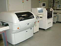
Two of the nine partners formed a cluster known as the Advanced Printing Group, and their aim was to form an integral partnership within the existing consortium. As a result, they specialised in being able to offer wafer bumping services to SME's, which use flip chip technologies and wafer level CSP packages in their products. With example products such as watches, pagers, cell phones, cameras and camcorders, the available technology has to exceed consumer expectations each time - every time. Hence solder paste stencil printing, electro-less Nickel/Gold and Palladium, and Gold electroplating had to be, and was achieved by the cluster partnership. More specifically, the partnership has been able to demonstrate an effective and economical method for wafer bumping with stencil printing of lead-free pastes. Lead-free stencil printing technology was therefore made a reality with wafer designs that had a minimum pitch of 200 microns for peripheral and area-array configurations. Stencil printing for type 6 pastes has yielded bump heights of 110 microns for area-array and peripheral structures. And with new developments in ultra fine pitch structures, type 7 pastes have yielded bump heights of just 45 microns. In addition, other test chips were assembled on FR4 assembly boards and can withstand thermal cycling of minus 55 to 125 degrees Celsius, and humidity levels of 85 percent at 85 degrees Celsius. These continual advances within the microelectronics industry for further miniaturisation means that flip chip and wafer packages are witnessing increased utilisation in consumer electronics. Thus and with the continuing market explosion of consumer communication devices, it is expected that lead-free interconnections should be able to sustain a healthier utilisation demand well into the future.