Raman spectroscopy for more reliable microelectronics
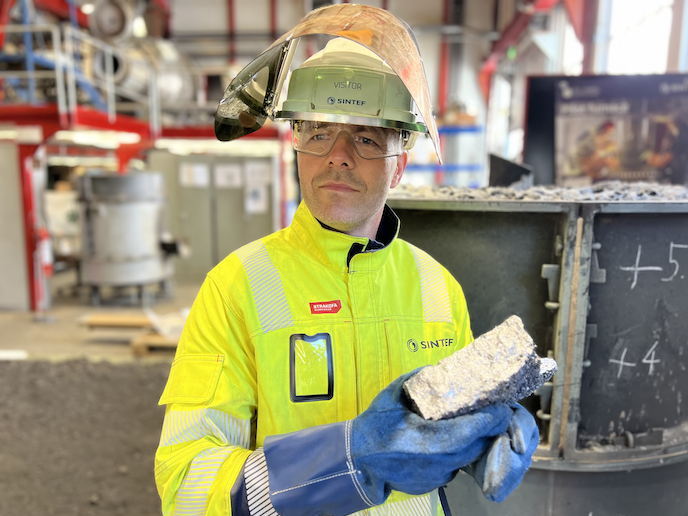
Mechanical stress is an important concern for the processing and reliability of electronic microsystems. Local mechanical stress occurs during nearly all stages of their processing and packaging. These stresses may affect the functionality of the chip and should therefore be controlled. Micro-Raman spectroscopy (µRS) is a non-destructive technique that makes use of the interaction of monochromatic laser light that is focused through a microscope, with lattice (phonons) or molecular vibrations. However, the spatial resolution of most common instruments is, at its best, about 1mm. The STREAM project developed a system that advances this technique. Within the framework of the STREAM project, the sensitivity of µRS to local strain in the lattice aimed to be used for microelectronics processing. However, the increasing densification and miniaturisation of microelectronic devices demanded analytical techniques with spatial resolution even higher than the one that commonly used μRS may offer. In order to achieve improved spatial resolution, the conventional system is equipped with an auto focus, providing a constant focus of about 0.8 micron (458nm laser light, 100x objective). Moreover, the addition of an oil-immersion objective may improve the spatial resolution to 0.3 micron. These improvements make possible the use of the μRS technique in studies of microelectronics processing induced stress, with received data being comparable to data acquired with other methods, such as the Convergent-Beam Electron Diffraction (CBED) and the Finite Element Model (FEM). Since the field of microelectronics is growing very fast, there is an increasing demand for reliability assessment. µRS with the improvements described above could be used as an excellent tool for chips and microelectronic systems of even higher reliability and quality.