

Stencil printing advances the electronics industry
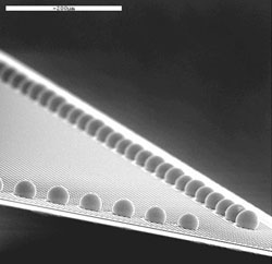
Current trends in the electronics industry for smaller, faster and importantly cheaper products have led to increased utilisation of advanced integrated circuit packages and accelerated adoption of flip chip technologies. In particular, the attractiveness of flip chip technologies lies in their superior electrical performance, higher thermal conductivity and input/output counts, which are all mandatory requirements for advanced semiconductor applications. Implementation of IZM’s Electroless Nickel/Gold plating for the deposition of under bump metallisation in conjunction with stencil printing of newly emerged Sn4%Ag0.5%Cu and Sn3.5%Ag lead-free pastes have rendered flip chip bumping technology a reality. This has brought about many accomplishments in the broad area of semiconductor packaging. Current research studies at Fraunhofer IZM/Technical University Berlin have demonstrated Ultra fine pitch bumping at pitches smaller than 120µm for peripheral chip pad arrays and up to 120µm for area pad arrays. Advanced very thin electroformed stencils (20µm in thickness) have been manufactured by IZM Industrial Partner with extreme care on foil expandability, roughness and stencil frame handling. Fraunhofer IZM has performed printing of UFP type 8 pastes and reflow soldering at 60µm pitch. The Feasibility studies on 6 inches wafers have yielded bump height of 28µm ± 3µm. UFP studies focus more importantly on innovative ultra fine pastes and new advancements in laser-cut and electroformed stencils which emerge as the only economical alternative for wafers with more than 50000 pads. As an alternative to stencil printing, technology researchers in Fraunhofer IZM are developing processes to print pastes in dry resists (Paste-in-Resist technology). Very advanced laminated resists up to 50µm in thickness can be lithographically opened to provide apertures for paste printing. By this technology route, paste release issues are no longer the determining factor for bump uniformity and yield. Subsequent reflow soldering yields high quality bumps of any desirable tin-lead or lead-free composition on electroless Ni/Au UBM pads. Paste-in-Resist technology has the potential to extend further down the Ultra fine pitch limits of the conventional stencil printing. It also offers the advantage of bumping wafers with various ternary lead-free compositions and therefore complementing conventional electroplating bumping technologies. Caption: Lead-free bumping at 60µm pitch