A portal to speed up silicon photonics tech development
The EU-funded photonixFAB(opens in new window) project has launched a new customer engagement portal providing early access to research and development and small-scale manufacturing for innovative product developers in the silicon photonics industry. This initiative is the project’s first step in its efforts to industrialise Europe’s silicon photonics value chain and provide a path to scalable high-volume manufacturing. The aim is “to elevate Europe’s global standing in silicon photonics,” a recent article(opens in new window) posted on the photonixFAB website reports. The project has brought together European partners spanning the entire photonics value chain, including technology and manufacturing service providers, application developers and major research organisations.
The path to engagement
The customer engagement portal is expected to play a key role in promoting early engagement with clients as the project progresses, enabling initial technology evaluations and consultations. This will make early product development possible “while the various technologies/services encompassed by photonixFAB are being transferred to an industrial environment over the course of 2024 to 2026.” Through the information offered on the different capabilities of the photonixFAB technology partners, the web-based platform provides users with the tools to decide which technologies or services they need. They are then directed to the relevant partners to initiate engagement. This gives customers a head start in developing their concept, creating prototypes and progressing to small-scale manufacturing.
Expertise on offer
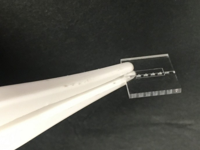
The technology partners’ expertise includes silicon-on-insulator (SOI) and silicon nitride (SiN) prototyping, as well as prototyping for indium phosphide (InP) chiplets. Packaging capabilities are also offered for both SiN and SOI processes, in addition to early technology access for InP micro-transfer printing on SiN and SOI. In addition, process design kits are available through the technology partners. Photonic Program Manager Youssouf Guerfi of photonixFAB project coordinator X-FAB, France, discusses the portal’s important role in promoting silicon photonics in Europe: “Substantial progress is already being witnessed on photonixFAB, with valuable contributions being made by all of the consortium members. The customer engagement portal is an important milestone in our ongoing journey with this initiative. Using the portal, customers will be able to find the correct partners and start carrying out the preliminary stages of their photonic projects, to be ready to benefit from full-scale production in the future.” X-FAB Business Line Manager for Photonics Joni Mellin adds: “We are seeing a great deal of interest in the European-based silicon photonics value chain that photonixFAB represents. This launch signifies that we are now open for business and projects can get underway, so no time is wasted. It means that we can accelerate engagement activity and customers can get ahead of the game.” The photonixFAB (Building a European industrial supply chain for SOI- and SiN-based silicon photonics, including heterogeneous integration to support emerging markets) project ends in 2026. For more information, please see: photonixFAB project website(opens in new window)


