Prediction of strain and stresses on the micron-metre scale
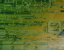
Considering the enormous market growth and the advanced application requirements, microelectronics are continuously searching for miniaturisation of their devices by introducing new fabrication methods and materials. This ever-increasing miniaturisation has tremendous impact on the mechanical systems of integrated circuit, with mechanical stresses being the most prominent. Their adverse effects on silicon characteristics may also affect the performance and the life cycle of microsystems. Motivated by this, this project developed a software prototype for simulating the stress induced by a variety of technological processes used in the fabrication of silicon-based microelectronics devices. The so-called IMPACT is a 2D process simulator, capable of predicting stresses affecting silicon technology and in particular those caused by extrinsic sources such as water diffusion and phase transformation. The tool has been developed with Fortran 77 and 90 and uses the Finite Element Method to discrete the physical models. Within this project, models related to the calculation of stresses and strain during the manufacturing of the devices have been improved. In particular, the highly complicated rheological behaviours of thin film materials, such as viscoelastic and elasto-plastic laws, have been implemented and calibrated. The tool has been validated with 0.15-micron test structures for non-volatile memory applications, such as ROM devices. The provider is looking for collaboration with technology developers/manufacturers of silicon technologies, including CMOS/BICMOS/Bipolar technologies for improving and adding new models. In addition, collaboration is also sought with a software house for adding a graphical user interface and low level interactive documentation for further commercialisation of the tool.