Incompatible wafer bonding materials made compatible
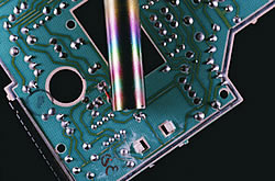
The bonding of wafers in the Microelectronics industry is used for the manufacture of microsystems and silicon-on-insulator materials. Current bonding processes require wet chemical activation and high temperatures, with some extremes reaching 1000 degrees Celsius. Temperatures of this magnitude mean that certain metallic compositions cannot withstand the manufacturing processes, thus minimising potential optimisation. Taking into account the high temperature limitations a Swedish university has investigated pure room silicon wafer bonding processes. This process employs the sputtering and evaporation technique, where the wafer surfaces are exposed to oxygen, nitrogen or argon plasma gases. The process ionises the gas into a collection of charged particles so that when the plasma is directed at the metallic target, the material can be deposited on to a silicon wafer. The results of this innovative process means that mechanical and electrical structures of different melting temperatures can be merged into a single stable component; and all done at room temperature. The experiments also revealed that N-type (100) silicon; silicon dioxide and crystalline quartz exhibit high surface energies equivalent to conventional high temperature annealing techniques. Microsystem manufacturing is the primary application theatre, but the researchers foresee potential applications in all aspects of the microelectronics industry. The university is currently conducting further research and would be interested in further development support and licence agreements.