Leading to ultra-precision silicon etching
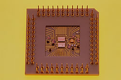
The rapid evolution of on-chip integrated sensors has imposed ever-increasing needs in their fabrication techniques. Sensing elements are normally determined after circuit fabrication allowing the use of standard technologies such as CMOS and the reduction of the required wafer processing. In order to satisfy the needs of MEMS manufacturing industry a large diversity of the techniques and instruments are offered. Silicon etching is typically used for structure definition with precision etching being more suitable for the design of smaller components, paying particular attention to profile verticality and sidewall smoothness. These methods are commonly employed in Micro-Opto-Electro-Mechanical Systems (MOEMS) applications (fibre optic switches, projection displays, integrated optical sensors) and embossing die systems (ink jet print heads). Although wet etching processes are rapid and inexpensive, they are difficult to use in specialised situations including fabrication of micronozzles for ink-jet print heads. This is mainly because they feature isotropy in etching and/or present crystal planes as facets within silicon. In order to overcome these shortcomings, the FUPUSET project investigated the kinetics and mechanism of chemical and electrochemical dissolution of silicon in an aqueous environment. Taking advantage of the recent advancements in instrumentation and studies on physical chemistry of semiconductor electrodes, the project improved the surface finish of micro machined components. This was due to the inclusion of a novel process step that reduces the surface roughness without deteriorating the anisotropic ratio during etching. In addition, anisotropic ratios were also improved by proper selection of design parameters such as the electrochemical potential during etching. Moreover, surface finish and anisotropic ratio of etched silicon were found to be inversely related. Depending on the final product, a compromise between these two parameters has to be made during the anisotropic etching process. Nevertheless, the undesirable effects of a strong anisotropy including micro-pyramids formation, may be removed with the aid of oxidants at the end of the etch while improving the surface finish.